Key Points
- A naturally formed p-n junction just 3.3 nm thick was discovered in MnBi₆Te₁₀. The junction formed unexpectedly during quantum material research.
- Uneven electron distribution created internal electric fields, acting like semiconductor junctions.
- These junctions are highly light-sensitive and could power future spintronic devices.
- The discovery may complicate some quantum computing plans but opens new avenues in electronics.
In a breakthrough that could reshape the future of nanoelectronics and quantum devices, scientists have discovered that a quantum material can naturally form one of the thinnest semiconductor junctions ever observed — just 3.3 nanometers thick, nearly 25,000 times thinner than a sheet of paper.
Researchers from the University of Chicago Pritzker School of Molecular Engineering (UChicago PME) and Pennsylvania State University were studying the electronic behavior of MnBi₆Te₁₀, a topological material with quantum properties. These materials allow electricity to travel along their edges without resistance, making them highly promising for next-generation computing.
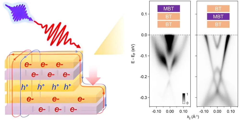
The team infused MnBi₆Te₁₀ with antimony, aiming to create a charge-neutral quantum material. While standard tests confirmed neutrality, a closer look using ultrafast laser-based trARPES (time- and angle-resolved photoemission spectroscopy) revealed something unexpected: electrons were unevenly distributed within the crystal’s atomic layers. This unevenness created tiny internal electric fields, mimicking naturally occurring p-n junctions — key components in semiconductors used in nearly all electronic devices.
“This was a big surprise,” said Asst. Prof. Shuolong Yang. “We weren’t trying to make this junction, but the material made one on its own.”
These self-forming p-n junctions offer a pathway to ultra-miniaturized electronics and respond strongly to light, making them potentially useful in spintronics. This technology leverages an electron’s spin rather than charge for data storage.
The phenomenon is believed to result from atomic swapping between manganese and antimony, which causes internal charge differences. Though this could complicate some quantum computing applications, it opens the door to new functionality in electronics and photonics.
The UChicago team is now working on thin-film versions of MnBi₆Te₁₀, aiming for better control over the material’s electronic behavior and greater device scalability. “This is the beauty of basic research,” said Yang. “We aimed for one goal and discovered something that could change everything.”


