
Key Points:
- Intel unveils an ambitious semiconductor roadmap, including introducing a 14A node for 1.4 Nanometer technology.
- Faces competition from TSMC, which plans to commence volume production of 2nm chips by 2025.
- Based on GAA nanosheet transistor architecture, TSMC’s 2nm technology promises to be the most advanced.
- Intel aims to become the world’s second-largest foundry by 2030, focusing on AI-driven chip design.
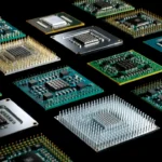
In a strategic move to reclaim its semiconductor chip manufacturing leadership from Asian rivals, Intel revealed its new technology roadmap at the Intel Foundry Direct Connect event on Wednesday. The highlight of the announcement was the introduction of the Intel 14A node, marking Intel’s foray into 1.4 Nanometer technology and providing insights into its roadmap beyond 2025.
Intel CEO Pat Gelsinger emphasized the significance of the 14A node, outlining Intel’s plans to begin productionizing 18A this year and the newly unveiled 14A node around 2027. The roadmap also includes advancements for Intel 3 and Intel 18A, with Intel 3-T optimized for 3D advanced packaging designs and nearing manufacturing readiness.
While Intel aims to regain its technology leadership by 2025 with 18A, it faces stiff competition from TSMC, the world’s largest contract chipmaker. TSMC has confirmed plans to commence volume production of 2nm chips by 2025, positioning itself as a frontrunner in deploying advanced technology. TSMC’s 2nm technology, based on GAA nanosheet transistor architecture, promises to be the most advanced upon its introduction in 2025.
Moreover, TSMC asserts that its enhanced 3nm technology will offer comparable performance to Intel’s 18A chip while enjoying advantages in time-to-market, technology maturity, and cost structure. With TSMC and Samsung already producing 3nm chips, Intel faces pressure to catch up, as all three companies target the production of 2nm chips by 2025.
During the event, Gelsinger also announced the launch of the ‘world’s first systems foundry for the AI era,’ reaffirming Intel’s commitment to becoming the world’s second-largest foundry by 2030. He highlighted the transformative impact of AI on technology and emphasized the partnership opportunities for chip designers through Intel Foundry.
In a significant development, Microsoft chose Intel’s 18A process to manufacture a chip design, solidifying Intel’s position as a key player in the semiconductor industry. Microsoft’s decision underscores the confidence in Intel’s technology and aligns with Intel’s ambition to drive innovation in chip design and manufacturing.