
Key Points:
- Samsung secures its first contract for 2-nanometer node AI chip production from Preferred Networks Inc. (PFN).
- The collaboration allows PFN to access Samsung’s cutting-edge chip technologies, enhancing its competitive position.
- Samsung gains a crucial customer for its most advanced chip technology, strengthening its position against TSMC.
- Samsung’s 2-nanometer technology, based on GAA transistor architecture, will be applied to HPC chips and automotive chips in the coming years.
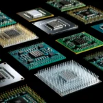
Samsung Electronics, the global leader in memory chip manufacturing, has achieved a significant milestone by securing its first contract to produce artificial intelligence (AI) chips using cutting-edge 2-nanometer node technology. The contract comes from Japanese startup Preferred Networks Inc. (PFN), marking a notable victory for Samsung over its competitor, Taiwan Semiconductor Manufacturing Co. (TSMC), in the race for advanced chip processing technology.
Under the agreement, Samsung will leverage its latest 2-nanometer chip processing technology to manufacture AI accelerators and other AI chips for PFN. This marks a departure for PFN, which had collaborated with TSMC since 2016 but opted for Samsung’s 2-nanometer node for its next-generation AI chips.
The mutually beneficial partnership provides PFN access to Samsung’s cutting-edge chip technologies, enhancing its competitive edge. Simultaneously, Samsung gains a significant customer for its most advanced chip technology, positioning itself favorably against TSMC in the foundry market.
Preferred Networks Inc. (PFN), established in 2014, specializes in AI deep learning development and has attracted substantial investments from major companies, including Toyota Motor, NTT, and FANUC, a Japanese robot system maker.
While TSMC currently boasts more clients for its 2-nanometer technology, PFN’s decision to collaborate with Samsung could signal a shift in Samsung’s favor. Industry analysts believe this move might open doors for Samsung to secure additional important clients in the competitive chip manufacturing landscape.
Samsung’s 2-nanometer technology, based on Gate-All-Around (GAA) transistor architecture, is set to be applied to high-performance computing (HPC) chips for supercomputers and computer clusters in 2026, followed by automotive chips in 2027. The company plans to mass-produce more advanced 1.4-nanometer chips by 2027.
The competition between Samsung and TSMC in advancing chipmaking processes is intensifying, with both companies aiming for technological supremacy in the coming years. Samsung’s Chief of Device Solutions, Kyung Kye-hyun, expressed confidence that the company would overtake TSMC within the next five years with its advanced GAA technology.
Samsung’s stride into 2-nanometer chip production signifies a pivotal moment in the race for semiconductor innovation, emphasizing the company’s commitment to pushing technological boundaries and meeting the rising demand for high-performance chips.