

In the vast realm of nanotechnology, nanopatterning is a groundbreaking technique that enables the precise manipulation of matter at the molecular and nanoscale levels. By harnessing advanced fabrication methods, nanopatterning enables scientists and engineers to create intricate patterns and structures with dimensions measured in nanometers. This article delves into the realm of nanopatterning, exploring its principles, techniques, and transformative applications across diverse fields of science and technology.
Exploring Nanopatterning
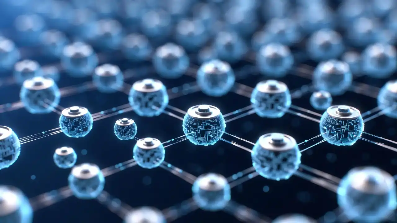
Nanopatterning involves arranging nanoscale features on surfaces, substrates, or materials to achieve specific functionalities or properties. This process requires precise control over nanostructure size, shape, orientation, and arrangement, often using sophisticated fabrication techniques and tools.
Principles of Nanopatterning
At its core, it relies on principles of lithography, self-assembly, and directed assembly to create patterns and structures at the nanoscale:
- Lithography: Lithographic techniques, such as photolithography, electron-beam lithography, and nanoimprint lithography, use masks or templates to selectively expose or remove material from a substrate, creating patterns with nanometer-scale resolution.
- Self-assembly: Self-assembly methods exploit the inherent properties of certain materials to organize into ordered structures at the nanoscale spontaneously. Examples include block copolymer self-assembly and DNA origami, where molecular interactions drive the formation of precise nanostructures.
- Directed Assembly: Directed assembly techniques involve guiding and manipulating individual nanoscale building blocks into desired configurations using external stimuli or forces. These methods enable precise control over the arrangement of nanostructures, such as nanowires, nanoparticles, and carbon nanotubes.
Techniques of Nanopatterning
A variety of techniques are employed in nanopatterning to achieve precise control over nanostructure placement and arrangement:
Top-Down Approaches
Top-down approaches involve fabricating nanostructures by selectively removing material from a larger substrate using lithographic methods. Examples include electron beam lithography, focused ion beam milling, and atomic force microscopy-based patterning, which enable high-resolution patterning with nanometer-scale precision.
Bottom-Up Approaches
Bottom-up approaches rely on the self-assembly or directed assembly of nanostructures from molecular or atomic building blocks. Techniques such as molecular beam epitaxy, chemical vapor deposition, and nanoparticle synthesis enable the controlled growth and deposition of nanostructures with atomic-scale precision.
Applications of Nanopatterning
Nanopatterning finds widespread applications across various fields, driving innovation and enabling transformative technologies:
Nanoelectronics and Photonics
In nanoelectronics and photonics, it is crucial to fabricate nanoscale devices, such as transistors, diodes, and photonic components. Shrinking device dimensions to the nanoscale enables faster, smaller, and more energy-efficient electronic and optical systems.
Nanomedicine and Biotechnology
In nanomedicine and biotechnology, it facilitates the development of advanced drug-delivery systems, biosensors, and tissue-engineering scaffolds. Nanostructured surfaces and interfaces created through techniques offer precise control over biomolecular interactions, enabling targeted drug delivery, sensitive diagnostics, and regenerative therapies.
Nanomaterials and Surface Engineering
Nanopatterning plays a crucial role in tailoring the properties of nanomaterials and engineered surfaces for various applications. Controlling surface roughness, wettability, and functionality at the nanoscale allows techniques to improve catalysis, energy storage, and anti-fouling coatings.
Future Directions and Challenges
Despite its tremendous potential, it faces several challenges and opportunities for further advancement:
Scalability and Throughput
Scaling up nanopatterning techniques to accommodate large-area patterning and high-volume manufacturing remains a significant challenge. Improving throughput, reducing fabrication costs, and enhancing the scalability of nanopatterning processes are essential for widespread adoption in industry and commercial applications.
Multidisciplinary Collaboration
Addressing the complex challenges of nanopatterning requires multidisciplinary collaboration among scientists, engineers, and researchers from diverse fields. By fostering interdisciplinary partnerships and knowledge exchange, researchers can accelerate innovation, overcome technical barriers, and unlock new opportunities for nanopatterning in emerging fields.
Novel Materials and Fabrication Techniques
Continued research into novel materials and innovative fabrication techniques is essential for advancing capabilities. Exploring new materials with unique properties, developing novel patterning methods, and refining existing techniques will drive progress in nanopatterning and open new avenues for scientific discovery and technological innovation.
Conclusion
Nanopatterning stands at the forefront of nanotechnology, offering unprecedented control over matter at the atomic and molecular scales. From nanoelectronics and photonics to nanomedicine and biotechnology, nanopatterning fuels innovation across diverse fields, driving the development of advanced materials, devices, and systems with unparalleled performance and functionality. As researchers continue to push the boundaries of nanopatterning technology, the transformative impact of precise nanoscale manipulation promises to reshape industries, revolutionize technologies, and unlock new frontiers of scientific exploration.