Key Points:
- An international research team led by the University of Göttingen demonstrates the light-like behavior of electrons in double-layer graphene.
- Double-layer graphene combines high electron mobility with insulating properties, essential for transistor functionality.
- Electric field manipulation toggles the conductivity of double-layer graphene, offering the potential for energy-efficient transistors.
- Breakthrough opens avenues for exploring bilayer graphene’s potential in transistor technology and other technological applications.
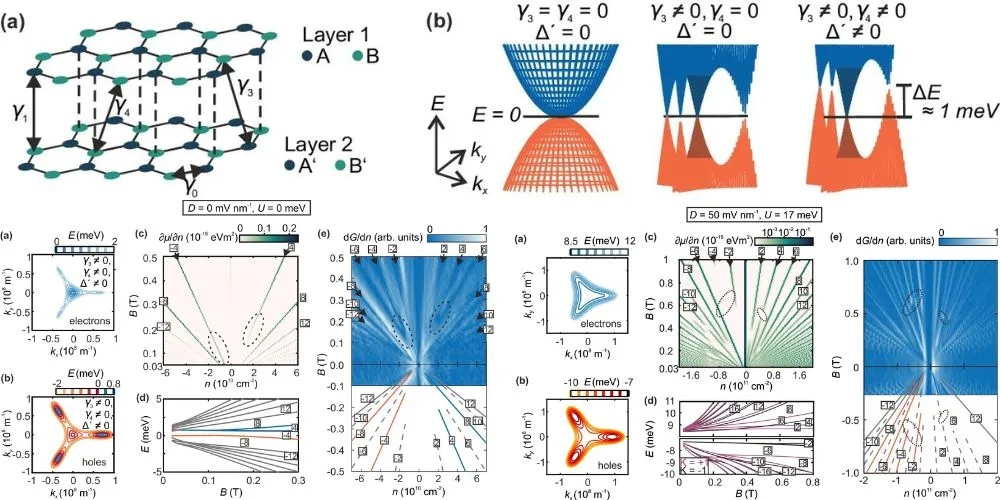
An international research team, spearheaded by the University of Göttingen, has achieved a groundbreaking milestone in graphene research, shedding light on the extraordinary behavior of electrons in naturally occurring double-layer graphene. Their experimental findings, published in Nature Communications, unveil a remarkable phenomenon where electrons in graphene exhibit properties akin to massless particles, resembling the behavior of light. Moreover, the researchers have demonstrated the ability to manipulate the flow of current, akin to flicking a light switch, with implications for developing minuscule and energy-efficient transistors at the nanoscale.
Graphene, a single layer of carbon atoms, was first discovered in 2004 and is renowned for its exceptional electrical conductivity, attributed to the rapid movement of electrons within the material. Scientists have long envisioned leveraging graphene’s properties to create faster and more energy-efficient transistors. However, the challenge lies in achieving highly conductive and insulating states within the material, a prerequisite for transistor functionality. Traditional graphene lacks an insulating state, limiting its potential for transistor applications.
The breakthrough emerged when the Göttingen University team investigated double-layer graphene, composed of two graphene layers. This naturally occurring configuration combines the benefits of high electron mobility akin to light propagation with the insulation capacity. By applying an electric field perpendicular to the material, the researchers could toggle the conductivity of double-layer graphene, rendering it insulating. This transformative property, theoretically proposed in 2009, was realized through enhanced sample quality facilitated by materials provided by NIMS and collaborative efforts with MIT.
The experiments, conducted at cryogenic temperatures, underscore the potential of bilayer graphene to revolutionize transistor design, offering the promise of highly efficient electronic components. Professor Thomas Weitz from Göttingen University’s Faculty of Physics remarks on the significance of the findings, emphasizing the team’s excitement in validating the theoretical predictions through empirical evidence. Dr. Anna Seiler, the study’s first author, underscores the pivotal nature of their work as an initial step toward harnessing the potential of bilayer graphene in transistor technology and beyond.
The research marks a significant stride in graphene science, unlocking new possibilities for ultra-efficient transistors and advanced technological applications. With further exploration and development, bilayer graphene holds the potential to catalyze innovation across various domains, propelling advancements in electronics and beyond.


