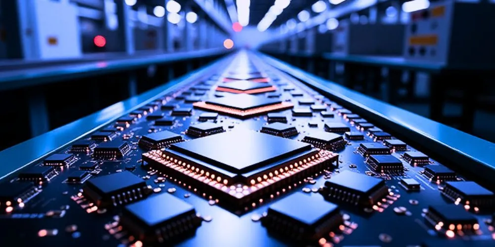
Semiconductor foundries, also known as fabs, are key elements in the modern electronics industry. They serve as specialized factories where integrated circuits (ICs) are manufactured and assembled. These facilities are essential for the production of microchips that power everything from smartphones and laptops to automotive systems, AI platforms, and the Internet of Things.
Role and importance of semiconductor foundries
Semiconductor foundries are manufacturing facilities that produce chips based on designs provided by other companies. This model, known as the “foundry model,” emerged in the 1990s and has since become the dominant approach in the industry. Companies that design chips but do not manufacture them are called fabless semiconductor companies that rely on foundries to turn their designs into physical devices. Meanwhile, foundries focus on perfecting manufacturing processes, investing in advanced equipment, and achieving economies of scale that make large-scale chip production feasible and cost-effective.
Foundries are essential for driving innovation because they enable companies to access state-of-the-art manufacturing capabilities without the prohibitive costs associated with building and maintaining their fabrication plants. This is particularly important as the price of building a new fabrication facility (fab) routinely exceeds several billion dollars.
AI, EVs, and IoT fuel demand for customized semiconductor solutions
Semiconductor foundries are no longer limited to producing general-purpose processors. The rapid growth of AI, 5G, automotive electronics, and IoT is driving demand for specialized chips tailored to specific applications. The rapid expansion of AI and machine learning (ML) workloads is driving significant changes in the semiconductor manufacturing industry.
Foundries are increasingly focused on producing chips specifically designed for parallel processing, such as graphics processing units (GPUs), tensor processing units (TPUs), and application-specific integrated circuits (ASICs). These specialized chips are essential for handling the massive computational demands of AI in data centers, edge devices, and consumer electronics, enabling everything from real-time language processing to advanced image recognition.
At the same time, semiconductor foundries are responding to the evolving needs of the automotive, IoT, and high-performance computing sectors. In the automotive industry, the rise of electric and autonomous vehicles has led to a surge in demand for reliable, high-quality chips that can support battery management, sensor integration, and advanced driver-assistance systems. For IoT, foundries are developing low-power, highly efficient semiconductors that allow smart devices and industrial sensors to operate for extended periods with robust connectivity.
Meanwhile, the demand for faster and more energy-efficient data processing in cloud computing, scientific research, and enterprise IT is prompting foundries to innovate with chips that deliver greater computational power and reduced energy consumption.
How technology and sustainability define modern foundries
The semiconductor sector is rapidly advancing through innovations in manufacturing processes and chip design. Foundries like Samsung and Intel are widely adopting 2nm process nodes, enabling higher transistor density, improved performance, and lower power consumption. The adoption of Extreme Ultraviolet (EUV) lithography and now High-NA EUV systems allows for atomic-scale feature patterning, making ultra-dense chip architectures possible.
Meanwhile, 3D stacking and heterogeneous integration utilize technologies such as Through-Silicon Vias (TSVs) to combine multiple layers of logic and memory, resulting in more powerful, compact, and efficient chips. Gate-All-Around (GAA) transistors further boost efficiency and performance by offering superior current control compared to traditional FinFETs. According to Allied Market Research, the semiconductor foundry market is projected to grow at a CAGR of 8.1% from 2023 to 2032.
Additionally, chipset technology is revolutionizing processor design by integrating specialized silicon components at the package level, streamlining development, and improving yield. Across the manufacturing floor, AI and automation optimize layouts, enhance defect detection, streamline equipment maintenance, drive efficiency, and reduce downtime. Sustainability is also a growing priority, with foundries implementing green initiatives such as water reclamation, chemical recycling, and energy-efficient processes to minimize environmental impact and maintain a competitive advantage.
ASE to repurpose AMPI’s legacy tools
In May 2025, ASE Holdings, a global leader in semiconductor packaging and testing, announced that its subsidiary, ASE Test Limited, is expected to acquire Taiwan-based Advanced Microelectronic Products, Inc. (AMPI), a 6-inch wafer foundry. The move aims to restructure AMPI’s operations as part of a broader business overhaul.
Analysts believe that integration with ASE Holdings could enhance AMPI’s efficiency and scale, with potential privatization aimed at addressing ongoing losses. Through this acquisition, AMPI’s older fabrication tools are likely to be repurposed for compound semiconductor production or integrated into ASE’s packaging operations, supporting ASE’s vertical integration strategy and growing AI-driven market demands.
Final words
Semiconductor foundries are indispensable to the modern technology ecosystem. They enable the production of advanced chips that drive innovation in AI, automotive, IoT, and high-performance computing. Foundries are expected to meet the challenges and opportunities of the digital age in the coming years with ongoing investments in new fabs and continuous advancements in process technology, materials, and manufacturing techniques.


