In the dazzling world of modern technology, our attention is captivated by the finished product. We marvel at the computational power of NVIDIA’s latest AI chip, the seamless performance of Apple’s newest iPhone, and the vast data centers that power the cloud. These are the visible symbols of the digital age. But beneath this surface lies a universe of staggering complexity and profound importance: the world of semiconductor manufacturing. This is a realm of atomic-level precision, of cleanrooms thousands of times cleaner than a hospital operating room, and of machines so sophisticated they represent the very pinnacle of human engineering.
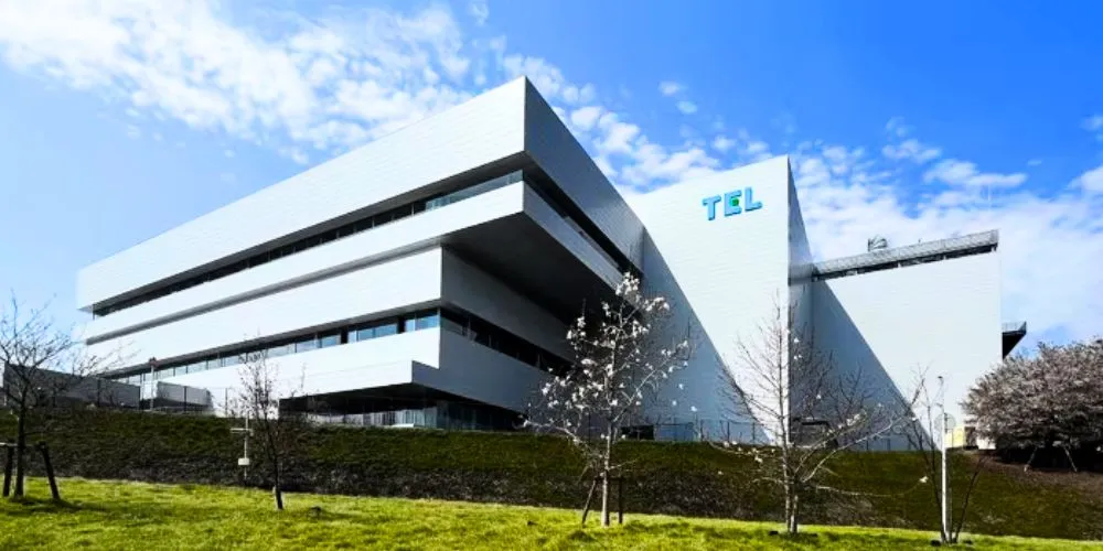
In this hidden world, there are a handful of indispensable giants, companies whose technology is so foundational that without them, the entire digital economy would grind to a halt. We may know the names of some, like the Dutch lithography titan ASML. But equally critical, yet far less well known outside the industry, is a Japanese powerhouse that has been a quiet and essential architect of the semiconductor revolution for 60 years. That company is Tokyo Electron Limited (TEL).
This is the definitive story of TEL, a company that rose from the ashes of post-war Japan to become one of the most dominant and profitable players in the semiconductor equipment industry. It is a tale of a shrewd transition from a technology trader to a world-class manufacturer, of a relentless focus on research and development, and of a corporate culture that blends Japanese precision with a uniquely global and customer-centric mindset. We will deconstruct TEL’s critical role in the chipmaking process, exploring its market-leading positions in coater/developers, etch systems, and deposition tools. We will trace its journey of growth, its legendary (and ultimately failed) merger with Applied Materials, and its crucial position at the heart of the geopolitical battle for semiconductor supremacy. This is the story of the invisible giant whose machines build the chips that build our world.
From Trading House to Tech Titan: The Genesis of Tokyo Electron
The story of Tokyo Electron does not begin in a research lab, but in the bustling world of international trade. Its origins are a testament to the unique circumstances of post-war Japan and the shrewd vision of its founders, who saw an opportunity to act as a bridge between a technologically resurgent Japan and the advanced electronics industry of the West.
The Post-War Japanese Electronics Boom
The 1950s and 60s were a period of miraculous economic recovery and growth for Japan. The country was rapidly transforming itself into an industrial powerhouse, with a particular focus on the burgeoning electronics industry. Companies like Sony and Panasonic were beginning to make a name for themselves. However, the Japanese industry still lagged behind the United States in advanced technologies, particularly in the nascent field of semiconductors.
Japanese companies were hungry for the latest American technology, but navigating the complexities of international trade and technology transfer was a significant challenge. This created an opportunity for a new kind of company: a specialized technology trading firm that could act as an importer and distributor of advanced foreign electronics.
The Founding by TBS and the Vision of a Trading Company (1963)
On November 11, 1963, Tokyo Electron Laboratories, Inc. was founded. It was established with a small amount of capital, largely provided by Tokyo Broadcasting System (TBS). The initial idea was to import and sell advanced foreign electronic products, such as professional audio equipment, to Japanese broadcasters like TBS. However, the company’s founders, Tokuo Kubo and Toshio Kodaka, had a grander vision. They were joined by a key figure, Ken Akahori, and the trio recognized that the biggest technological wave of the future was not in broadcasting, but in semiconductors.
They made a pivotal decision to focus the company on importing and selling highly specialized semiconductor manufacturing equipment. They traveled to the United States, the undisputed leader in semiconductor technology at the time, and began forging relationships with small, innovative American equipment startups.
The Partnership with Thermco: A Turning Point
A key early partnership that would shape the company’s destiny was with Thermco Products, an American manufacturer of diffusion furnaces. These furnaces are a critical piece of equipment used to heat silicon wafers to very high temperatures in a controlled atmosphere, a fundamental step in the chipmaking process.
TEL became the exclusive agent for Thermco in Japan. But TEL did more than just sell the machines. It provided meticulous after-sales service, maintenance, and technical support, building a deep level of trust with its Japanese customers. This customer-centric approach became a core part of TEL’s DNA. The company learned the intricacies of the equipment and, more importantly, the precise and demanding needs of Japanese chipmakers. This deep customer intimacy would prove to be an invaluable asset.
The Great Pivot: From Importer to Manufacturer
For its first two decades, TEL thrived as a trading company. It was highly profitable, acting as the gateway for American semiconductor equipment into the booming Japanese market. However, the company’s leadership knew that being a middleman was a strategically vulnerable position. To secure its long-term future and become a true technology leader, it had to make a bold, difficult pivot: transform itself from a technology importer into a world-class technology manufacturer.
The “All-Weather” Strategy: Diversification and R&D
This strategic shift was driven by a philosophy of building an “all-weather” company, one that could withstand the notoriously volatile and cyclical nature of the semiconductor industry. The leadership team knew that relying on a single product or a single foreign partner was too risky.
The transformation was executed through a two-pronged strategy. This approach allowed TEL to leverage its existing strengths while building new, powerful capabilities.
- Joint Ventures and Technology Licensing: Instead of starting from scratch, TEL’s first step was to form joint ventures with its foreign partners. A landmark move was the establishment of TEL-Thermco in 1968, a joint venture to begin manufacturing diffusion furnaces in Japan. This allowed TEL to gain invaluable manufacturing experience and to begin adapting the technology for the specific needs of the Japanese market.
- Investing in In-House R&D: Simultaneously, the company began to invest heavily in its own research and development. It started hiring top engineers and scientists and established dedicated R&D centers. The goal was not just to copy foreign technology, but to improve upon it and eventually develop its own proprietary, world-leading products.
The First Breakthrough: The Coater/Developer
The first major success of this new strategy came in a critical and highly complex area of the chipmaking process: photolithography. Photolithography is the process of “printing” the intricate circuit patterns onto a silicon wafer. While companies like Nikon and Canon were developing the “steppers” and “scanners” (the machines that project the circuit image), there is a crucial step that happens both immediately before and after this exposure: the application of a light-sensitive chemical called “photoresist” and the subsequent “developing” of the exposed pattern.
The machines that perform these steps are called “coater/developers” or “lithography tracks.” They are incredibly complex, requiring nanometer-level precision in coating thickness and uniformity. Building on its experience and R&D, TEL developed its own line of coaters/developers. Through relentless innovation and close collaboration with Japanese chipmakers, TEL’s machines became the best in the world. They were more reliable, more precise, and offered higher throughput than their competitors.
This was a monumental achievement. TEL had gone from selling someone else’s technology to becoming the undisputed global market leader in one of the most critical and technologically demanding segments of the semiconductor equipment industry. To this day, TEL commands a near-monopoly market share (around 90%) in the market for coaters/developers used in advanced chipmaking. This single product category became the bedrock of the company’s profitability and its reputation as a manufacturing powerhouse.
Building the Arsenal: A Deep Dive into TEL’s Core Technologies
Having established its dominance in coaters/developers, TEL systematically expanded its product portfolio, using its R&D prowess and deep customer relationships to become a leader in several other critical process steps. Today, the company is one of the very few “broadline” equipment suppliers in the world, offering a comprehensive suite of tools that cover a significant portion of the chip manufacturing workflow.
The semiconductor manufacturing process is a marvel of modern science, involving hundreds of sequential steps. TEL’s equipment is essential in four of the most important of these process areas.
Photolithography (Coater/Developers)
As discussed, this is TEL’s foundational market. Its CLEAN TRACK™ series of coaters/developers is the undisputed industry standard. These machines are massive, highly automated systems that seamlessly integrate with the lithography scanner (the multi-hundred-million-dollar EUV machines from ASML). The TEL track precisely coats the wafer with photoresist, shuttles it to the scanner for exposure, and then returns it for a post-exposure bake and developing process that reveals the circuit pattern. The precision required is staggering; any microscopic defect introduced at this stage would ruin the entire chip.
Etch Systems
After the circuit pattern is printed in the photoresist, the next step is to “etch” that pattern into the underlying silicon or other materials on the wafer. Etch systems are essentially atomic-scale sandblasters, using a combination of high-energy plasma and reactive gases to selectively remove material, carving the three-dimensional structures that form the transistors and wires of the chip.
Etching is an incredibly competitive and technologically difficult field. TEL competes directly with American giants like Lam Research and Applied Materials. TEL’s Tactrus™ and Etlan™ series of plasma etch systems have gained significant market share by offering leading-edge performance, particularly in the complex etching required for 3D NAND memory and advanced logic chips.
Deposition Systems
Deposition is the process of adding thin layers of material onto the wafer. These layers can be conductive (such as copper or tungsten for wiring) or insulating (such as silicon dioxide to separate the wires). There are several different types of deposition processes, and TEL has a strong position in a few key areas.
Here are the primary deposition technologies where TEL is a major player. These processes are fundamental to building up the complex, multi-layered structure of a modern chip.
- Thermal Processing (Diffusion Furnaces): This is a return to TEL’s roots. The company continues to be a leader in advanced vertical diffusion furnaces used for processes like oxidation (growing a layer of silicon dioxide) and annealing (heating the wafer to repair crystal damage).
- Chemical Vapor Deposition (CVD): In CVD, gases are introduced into a chamber and react on the wafer’s surface to form a solid film. TEL provides CVD equipment for a variety of applications.
- Atomic Layer Deposition (ALD): A more advanced technique that deposits material one single atomic layer at a time. ALD is essential for creating the ultra-thin, perfectly uniform films required for the most advanced transistors. TEL has a strong and growing position in this critical technology.
Wafer Cleaning Systems
Throughout the manufacturing process, the wafer must be cleaned hundreds of times to remove microscopic particles and chemical residues. Even a single speck of dust can destroy a multi-million-dollar chip. TEL provides a range of wet cleaning and surface preparation systems that use specialized chemistries to ensure the wafer surface is atomically clean before the next process step.
The TEL Way: A Unique Corporate Culture and Strategy
What has enabled TEL to succeed and thrive for sixty years in such a brutally competitive and technologically demanding industry? The answer lies in a unique corporate culture and a set of strategic principles that blend the best of Japanese manufacturing excellence with a global, customer-first mindset.
“Best Products, Best Technical Service”: A Customer-First Obsession
From its earliest days as a trading company, TEL learned that its success depended on providing impeccable service to its customers. This philosophy is encapsulated in its motto: “Best Products, Best Technical Service.”
TEL is renowned in the industry for its “field service engineers.” These are highly trained engineers who are permanently stationed inside their customers’ fabs (semiconductor fabrication plants). They work side-by-side with the chipmaker’s engineers, maintaining the TEL equipment, troubleshooting issues in real time, and gathering invaluable feedback. This deep, embedded relationship gives TEL an unparalleled understanding of its customers’ present and future needs, which directly informs its R&D roadmap. This customer intimacy is a powerful competitive advantage.
A Relentless Focus on R&D and Innovation
Moore’s Law defines the semiconductor industry, the relentless drive to make chips smaller, faster, and more powerful. To survive, an equipment company must be in a constant state of innovation. TEL consistently invests a significant portion of its revenue in R&D (often 10-15% or more). The company has a global network of R&D centers and actively collaborates with leading research consortia, universities, and, most importantly, its customers to develop the next generation of process technologies.
A Disciplined Financial and Operational Model
Like many successful Japanese industrial companies, TEL is known for its strong operational execution and disciplined financial management. The company maintains a very strong balance sheet, with a high cash position and low debt. This financial strength allows it to continue investing heavily in R&D even during industry downturns, ensuring that it is ready with the latest technology when the next upcycle begins. This long-term perspective is a key reason for its enduring success.
A Tale of a Failed Merger: The Applied Materials-TEL Deal
One of the most dramatic and consequential events in TEL’s modern history was its attempted “merger of equals” with its largest American rival, Applied Materials (AMAT). The story of this failed mega-deal is a fascinating case study in business strategy, corporate culture, and the growing influence of geopolitics on the technology industry.
The Strategic Rationale: Creating an Unstoppable Behemoth
In 2013, AMAT and TEL, the number one and number three players in the semiconductor equipment market, respectively, announced a stunning $29 billion merger. The strategic rationale was incredibly compelling.
The proposed merger would have created a company with an unparalleled product portfolio and market position. The combination was seen as a way to tackle the soaring costs of R&D and to create a more efficient, powerful partner for the world’s leading chipmakers.
- Complementary Product Portfolios: While there was some overlap, the two companies were highly complementary. AMAT was a leader in deposition and ion implantation, while TEL was dominant in coaters/developers and had a strong position in etch. The combined company would have a commanding market share in nearly every major process step.
- Scale and R&D Synergies: The cost of developing the next generation of equipment for new, smaller chip nodes was skyrocketing. By combining their massive R&D budgets, the new company could accelerate innovation and tackle these challenges more effectively.
- Global Reach: The combination of AMAT’s strength in the U.S. and TEL’s deep roots in Japan and Asia would create a truly global powerhouse.
The Collapse of the Deal: Regulatory and Geopolitical Hurdles
The deal was incredibly complex, involving two industry giants with different corporate cultures and home countries. However, the ultimate undoing of the merger came from regulatory opposition. Antitrust regulators in several countries were concerned that the combined company would have too much market power, potentially stifling competition and leading to higher prices for chipmakers.
The final nail in the coffin came from the U.S. Department of Justice and, crucially, from Chinese regulators. The Chinese government, which was in the early stages of its own massive push to build a domestic semiconductor industry, was particularly concerned that the merger would create a single, dominant foreign supplier with immense leverage over its fledgling chipmakers. In April 2015, after failing to secure approval from all required regulators, the two companies announced they were abandoning the merger.
The Aftermath: A Blessing in Disguise?
While the merger’s failure was a major disappointment at the time, in hindsight, it may have been a blessing in disguise for TEL. The company received a significant break-up fee from AMAT. More importantly, it was forced to chart its own independent course. The experience seemed to energize the company, leading to renewed focus on its own R&D and a successful drive to gain market share against rivals. In the years following the failed merger, TEL’s financial performance and stock price have soared, and it has solidified its position as one of the indispensable “big three” of the semiconductor equipment world, alongside ASML and Lam Research.
At the Heart of the Chip War: TEL’s Geopolitical Significance
In recent years, the semiconductor industry has moved from the business pages to the front pages, becoming a central battleground in the escalating strategic competition between the United States and China. As one of the handful of companies that produce the most advanced chipmaking equipment, TEL finds itself in a powerful yet precarious position.
The U.S. Export Controls on China
The U.S. government has identified semiconductors as a critical national security technology. To slow down China’s military modernization and its progress in advanced technologies like artificial intelligence, the U.S. has implemented a series of sweeping export controls designed to cut off China’s access to the most advanced chips and, crucially, the equipment used to manufacture them.
While the U.S. leads these controls, their effectiveness depends on the cooperation of other key countries that possess critical chipmaking technology. This has put immense pressure on the governments of the Netherlands (home to ASML) and Japan (home to TEL and other key suppliers, such as Nikon and Tokyo Ohka Kogyo).
Japan’s Alignment and the Impact on TEL
In 2023, the Japanese government, aligning with the U.S. strategy, announced its own set of export controls on advanced semiconductor manufacturing equipment. While the regulations did not explicitly name China, their scope was clearly designed to restrict the sale of cutting-edge tools to Chinese chipmakers.
This has had a direct and significant impact on TEL. China has historically been one of TEL’s largest and fastest-growing markets. The new restrictions mean that TEL is now prohibited from selling its most advanced equipment to many of its Chinese customers.
Here’s how this geopolitical reality is reshaping TEL’s business and strategy. The company must now navigate a world where national security concerns are bifurcating its market.
- Loss of a Major Growth Market: The restrictions on sales to China represent a significant headwind, cutting the company off from a large portion of its potential market for advanced tools.
- Increased Demand from “Friend-Shoring”: On the other hand, the global push to diversify semiconductor supply chains away from China and Taiwan is creating a massive new wave of investment in fab construction in the United States, Europe, and Japan. This “friend-shoring” trend is a major tailwind for TEL, as these new fabs will all need to be filled with its equipment.
- Navigating a Complex Regulatory Landscape: The company’s leadership must now be as adept at geopolitics and trade law as they are at engineering. Navigating the complex and shifting web of international export controls has become a critical part of the business.
TEL’s position highlights the new reality for the global technology industry: it is no longer possible to be a purely commercial actor. The world’s most advanced technology companies are now, whether they like it or not, strategic assets in a global geopolitical contest.
TEL’s Vision for the Future: “To be a truly global company that generates high added value and contributes to society.”
Looking ahead, TEL is focused on navigating the challenges of geopolitics while capitalizing on the semiconductor industry’s immense long-term growth drivers. The company’s strategy is built on several key pillars.
Driving the Technological Roadmap
The fundamental driver of TEL’s business is technological innovation. The company is investing heavily in the R&D needed to enable the next generations of chips. This includes developing new materials, new process technologies, and the equipment needed to manufacture the increasingly complex 3D chip architectures of the future, such as Gate-All-Around (GAA) transistors and vertical chip stacking (hybrid bonding).
A Commitment to Sustainability and ESG
Like all major industrial companies, TEL is placing a growing emphasis on Environmental, Social, and Governance (ESG) principles. The semiconductor industry is notoriously energy and resource-intensive. TEL is working to develop more energy-efficient equipment and new processes that reduce water and valuable raw material consumption. This is not just a matter of corporate responsibility; it is also a business imperative, as its customers are under increasing pressure to reduce the environmental footprint of their own operations.
Capitalizing on the AI and Data-Driven Era
The single biggest driver of semiconductor demand for the foreseeable future is the explosion of artificial intelligence. The massive data centers that train AI models and the devices that run them all require vast quantities of the most advanced logic and memory chips. This AI-driven demand is creating a supercycle of investment in new fab capacity, a direct and powerful tailwind for TEL.
Conclusion
The story of Tokyo Electron Limited is a powerful testament to the Japanese industrial virtues of long-term vision, meticulous execution, and a deep, almost obsessive, focus on quality and customer service. It is the story of a company that made a brilliant transition from a technology trader to a global manufacturing leader, not through flashy marketing or consumer-facing products, but through the quiet, relentless pursuit of engineering excellence.
TEL is a company that operates in a world of almost unimaginable precision, where success is measured in angstroms, and the margin for error is zero. Its machines, humming away in the pristine cleanrooms of the world’s most advanced fabs, are the unsung heroes of the digital revolution. They are the invisible hands that build the brains of our modern world, enabling everything from the smartphone in your pocket to the complex AI models that are reshaping our future.
In an era of increasing geopolitical tension, TEL’s role has become more critical and more complex than ever. It is no longer just a commercial enterprise; it is a strategic national asset and a key player in the global contest for technological supremacy. Its journey from a small trading house in post-war Tokyo to its current position as an indispensable pillar of the global semiconductor industry is one of the great, if underappreciated, success stories of modern business. The future will be built on silicon, and the machines that shape that silicon will, in large part, be built by the quiet giant from Tokyo.