

Key Points:
- Monash University researchers proved that adding controlled disorder to tiny optical devices actually improves their overall performance.
- The team created a device that integrates 11 different optical functions into one single, ultra-thin surface.
- Traditional optical design relies on perfect order, but this new mosaic pattern frees up space for multiple functions.
- This breakthrough could lead to smaller, lighter equipment for medical diagnostics, telecommunications, and space imaging.
Scientists usually hate disorder. Engineers spend entire careers trying to force materials into perfect, predictable patterns. However, researchers from the Monash University School of Physics and Astronomy just flipped this basic rule completely upside down. They discovered that deliberately introducing controlled disorder into ultra-thin optical devices makes them much more powerful. This surprising breakthrough allows a single tiny device to perform multiple complex tasks simultaneously.
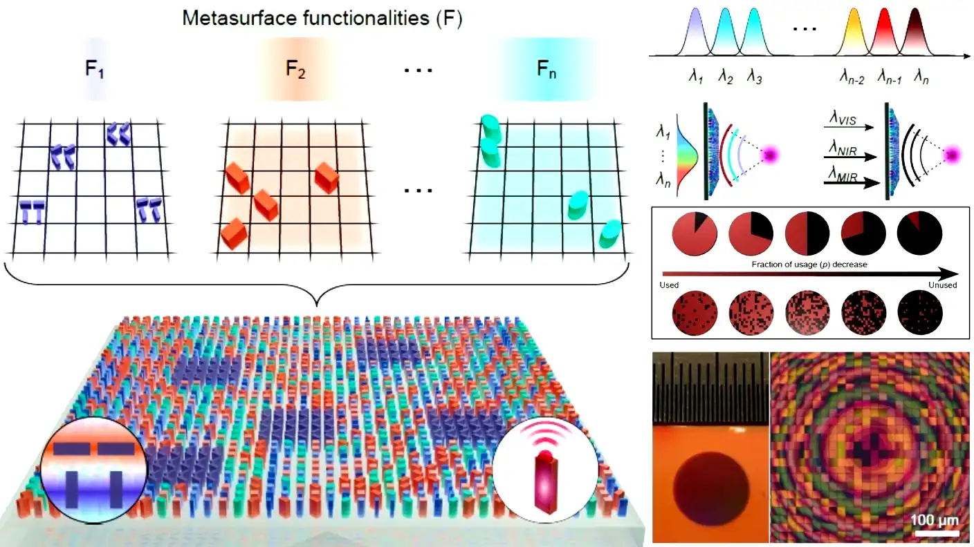
The research team recently published their findings in the journal Nature Communications. They introduced a brand new class of materials called disordered mosaic metasurfaces. These ultra-thin surfaces use nanoscale structures to manipulate light. The breakthrough centers on a very counterintuitive idea. Instead of carefully arranging these tiny structures in a perfectly repeating order, the team scattered them in a controlled mosaic pattern. They quickly found that the device performance did not drop at all. In fact, the scattered pattern improved the device’s performance.
Dr. Haoran Ren, a researcher from the Monash NanoMeta Group, explained the shift in thinking. He noted that engineers usually try to eliminate disorder. However, his team found that if you design the disorder carefully, it actually enhances what the devices can do. The scattered pattern allows scientists to pack far more functionality into the same physical space. This changes how researchers think about designing optical equipment.
Metasurfaces are ultra-thin arrays made up of tiny nanoscale structures. These surfaces already help reshape modern technologies, playing major roles in everything from medical imaging to complex quantum computing. But engineers have always faced one major limitation. Usually, each tiny device can only perform one specific function. If you need a device to do three things, you usually have to build three separate devices. This new disordered approach completely dismantles that old constraint.
Dr. Chi Li, the lead author of the study, explained how the mosaic layout works by comparing it to urban planning. He said traditional designs give the entire space a single function, much like a single massive building occupying a whole city block. The research team redesigned this tiny urban planning. By scattering the light-controlling elements, known as meta-pixels, they drastically reduced the physical area required for each function. This freed up space on the surface to embed additional capabilities. Multiple functions can now coexist efficiently without interfering with each other.
The team built a new type of optical lens to prove their concept worked. Usually, a lens that works across a broad range of light wavelengths requires bulky, complex camera systems. The Monash team integrated 11 distinct optical functions into one single, flat surface. This tiny device can focus light consistently across different colors without creating the visual distortion known as chromatic aberration. Most importantly, the team achieved this high performance without making the device bigger or more complicated to manufacture.
The researchers did not stop at building a better lens. They also demonstrated a powerful new way to capture images. The new metasurface can capture detailed information about how light polarizes, including complex light fields, in just one measurement. Before this discovery, scientists needed multiple measurements and heavy, specialized equipment to gather this specific data. The new device does it instantly. This opens the door to much faster, more compact optical sensors in the near future.
The real-world implications of this discovery span multiple industries. Companies constantly demand compact, multifunctional optical devices. When size and weight matter, this technology could change everything. The medical field could build smaller, more accurate diagnostic tools. Environmental scientists could deploy lighter sensors to track pollution. The telecommunications industry could improve fiber optic networks, and space agencies could launch smaller, more capable imaging satellites into orbit.
Dr. Li believes this platform provides the scientific community with a scalable way to integrate multiple optical functions into a single, compact device. He views this as a massive step toward creating truly multifunctional photonic systems. However, the biggest impact of this research might be conceptual. The team proved that engineered disorder can actually outperform perfect order. This simple fact challenges foundational assumptions across both photonics and general engineering.
Dr. Ren summed up the experience by saying that the most powerful innovations often come from questioning what we think we already know. By embracing disorder, his team unlocked capabilities that simply were not possible before. The team conducted the experimental work at the Monash Nanophotonics Laboratory, with extra help from researchers at the University of Exeter and the University of the Witwatersrand in South Africa.
Source: Nature Communications (2026).