
Key Points:
- Intel and 3DGS partnered with the Odisha government to build a massive $3.3 billion advanced packaging glass core substrate facility in India.
- Located in the Bhubaneswar-Khurda region, the project represents one of the largest high-technology manufacturing investments in India.
- The state-of-the-art facility will create over 1,800 direct high-skilled jobs and run in phases over the next five to six years.
- Utilizing glass substrates instead of traditional silicon, the plant will produce highly stable components for AI, 5G/6G, and defense.
India’s aggressive campaign to establish itself as a self-reliant global semiconductor hub has taken a massive, multi-billion-dollar leap forward. On Friday, May 29, 2026, the state government of Odisha, led by Chief Minister Mohan Charan Majhi, signed a landmark Memorandum of Understanding (MoU) with American chipmaker Intel Corporation and U.S.-based packaging pioneer 3DGS Inc. (3D Glass Solutions). The strategic agreement establishes a comprehensive framework to build a massive, state-of-the-art Advanced Packaging Glass Core Substrate Manufacturing Facility in India.
The proposed high-tech manufacturing plant represents one of the largest foreign direct investments in India’s semiconductor history. Located in the bustling Bhubaneswar–Khurda region, specifically within the high-tech Info Valley industrial park, the project has an estimated investment of $3.3 billion. The massive injection of capital will fund the construction of a vertically integrated facility combining substrate fabrication, component assembly, and advanced packaging under a single, highly optimized roof. The partners plan to build the facility in phases over a projected timeline of five to six years.
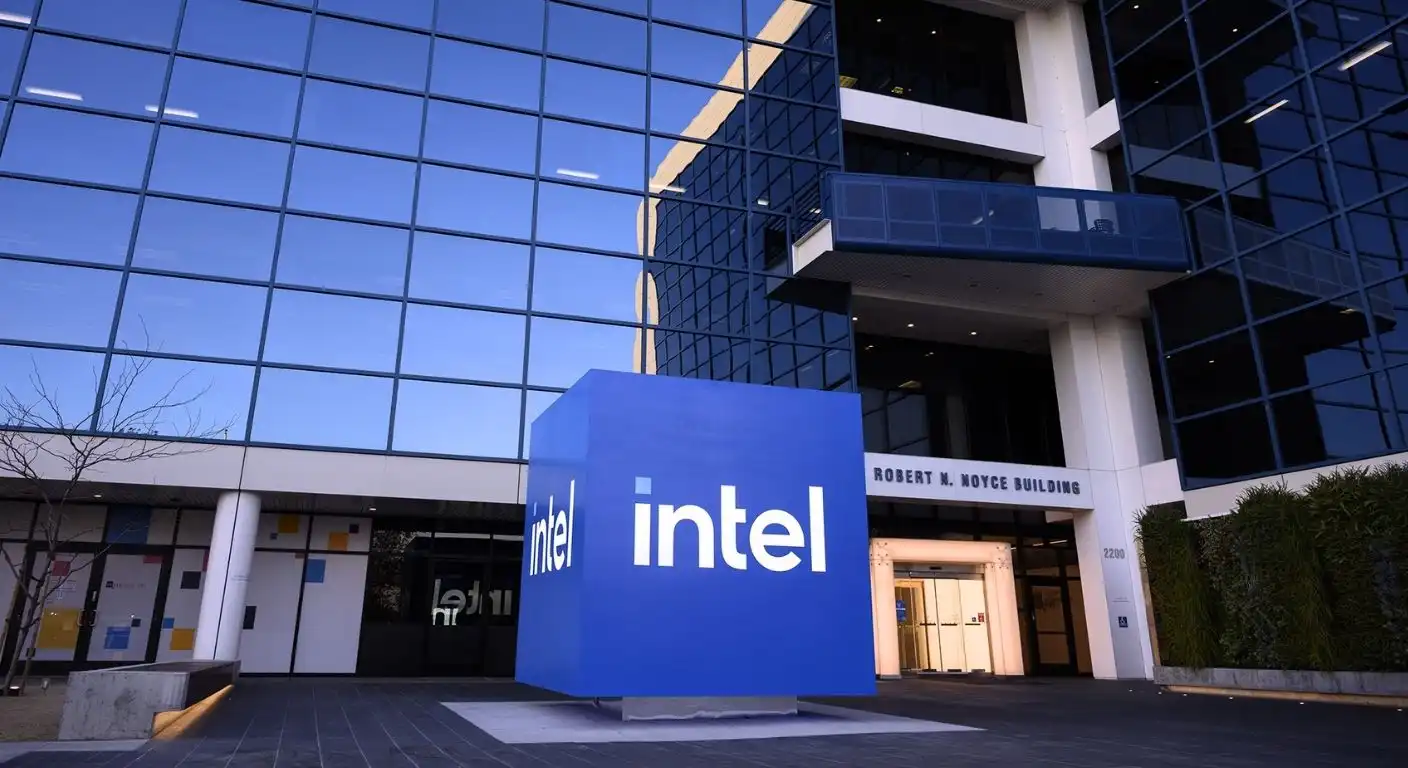
The landmark project marks the first major semiconductor initiative in India to feature the active, direct participation of chip major Intel. Under the terms of the agreement, Intel will provide critical technology expertise, process know-how, and engineering support to help 3DGS scale up production. Intel Capital has historically been a key institutional investor in 3DGS, having invested $8 million in the company across two prior funding rounds. By bringing its world-class process expertise directly to the Odisha project, Intel is helping India transition from simple assembly-led manufacturing toward deeper participation in the high-value, IP-intensive segments of the global semiconductor value chain.
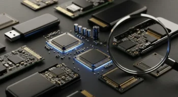
Technologically, the new facility represents a major leap beyond traditional silicon-based packaging methods. The plant will utilize 3D Glass Solutions’ proprietary APEX glass-ceramic packaging platform—protected by over 100 patents across 31 active patent families—to manufacture advanced glass-core substrates. Unlike conventional silicon substrates, glass-based substrates offer a significantly lower dielectric constant, superior high-frequency signal integrity, and exceptional thermal stability under heavy workloads. These physical advantages make glass substrates indispensable for next-generation applications, including artificial intelligence, 5G/6G communications, aerospace systems, and defense electronics.
The multi-billion-dollar development will also act as a major socioeconomic engine for eastern India. State officials estimate that the advanced packaging facility will generate more than 1,800 direct, high-skilled engineering and technical jobs, alongside thousands of indirect opportunities across the broader manufacturing and digital technology ecosystem. The growing semiconductor cluster will create large-scale employment opportunities for local engineering graduates, helping transform Odisha from a traditional, resource-based economy into a technology-led industrial growth center.
Union Minister for Electronics and IT Ashwini Vaishnaw praised the signing of the MoU, calling it a historic milestone for both Odisha and the nation. He emphasized that the entry of global technology leaders such as Applied Materials Inc., Lam Research, Tokyo Electron, and Merck Electronics—alongside the recent joint venture between Tata Electronics and the Dutch giant ASML—proves that the international chip industry places immense trust in India’s semiconductor ambitions. These coordinated investments align with the federal government’s Rs 76,000 crore India Semiconductor Mission (ISM) to build a resilient, self-sufficient chip ecosystem.
Odisha’s successful bid to host the $3.3 billion facility cements its growing reputation as India’s premier semiconductor hub. In addition to the 3DGS plant, the state had previously approved a major project by SiCSem Private Limited in collaboration with the UK’s Clas-SiC Wafer Fab. Located in the same Info Valley park, that facility will establish India’s first commercial compound semiconductor fabrication unit, focusing on high-efficiency Silicon Carbide (SiC) devices for electric vehicles, railways, and renewable energy. This means Odisha is now the only state in India hosting both a compound semiconductor fab and an advanced 3D glass packaging unit.
As the global semiconductor packaging market continues to grow rapidly—projected to exceed $100 billion by 2030—the transition to advanced packaging technologies has become a vital national security priority. By bringing 3D glass substrate manufacturing onshore, India is successfully reducing its heavy dependency on imported packaging technologies, which currently limits its technological sovereignty. If the joint venture completes its first phase and begins commercial production by August 2028, the project will put India at the cutting edge of global semiconductor tech, boosting its domestic chip manufacturing market share by an estimated 1.5% annually.