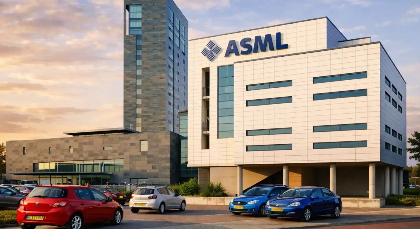
Europe’s most valuable technology company has delivered a blunt wake-up call to policymakers in Brussels. Executive leadership at Dutch semiconductor lithography giant ASML pointed out a stark industrial paradox: despite commanding an absolute global monopoly on the extreme ultraviolet machines required to manufacture the world’s most advanced microchips, the company generates virtually no leading-edge commercial sales within its home continent.
Speaking on the structural realities of the global semiconductor supply chain, company executives noted that European customers account for only about 1% of ASML’s total annual revenues. In sharp contrast, Asian manufacturing powerhouses—led by Taiwan, South Korea, and China—absorb more than 80% of total system shipments, with the United States capturing the vast majority of the remainder.
The massive geographic disconnect highlights the deep structural gap separating Europe’s geopolitical ambitions from its domestic industrial reality. While the European Union enacted the 43 billion euro European Chips Act to double the bloc’s share of global semiconductor manufacturing by 2030, the lack of advanced logic foundries, commercial memory gigafabs, and fast-track industrial permitting has left the continent as a minor player in the hardware revolution powering artificial intelligence.
The Stark Geographical Mismatch in Global Chipmaking
The commercial revenue breakdown of ASML provides an unfiltered map of where the modern digital economy is physically manufactured.
Asia Commands Eighty Percent of Lithography Deliveries
Advanced microchip fabrication is concentrated heavily in East Asia. Taiwan Semiconductor Manufacturing Co., South Korean memory leaders Samsung Electronics and SK Hynix, and domestic Chinese chipmakers purchase the vast majority of ASML’s annual manufacturing output.
During recent fiscal periods where ASML generated total annual net sales exceeding 32.7 billion euros and guided forward revenues toward 43 billion to 45 billion euros, Asian contract foundries and memory fabricators absorbed over 80% of all shipped lithography systems.
Taiwan and South Korea alone routinely account for more than 60% of quarterly system bookings. These Asian semiconductor titans operate massive fabrication clusters that run around the clock, deploying dozens of extreme ultraviolet machines in single cleanroom complexes to produce 3-nanometer logic chips, 2-nanometer prototypes, and high-density High Bandwidth Memory stacks.
Because East Asian governments provide streamlined environmental approvals, abundant water and high-voltage power infrastructure, and deeply integrated supplier networks, chipmakers continue to concentrate their capital expenditures in Asian science parks.
European Sales Languish Near One Percent of Global Revenue
In stark contrast to the massive shipments flowing eastward, ASML’s sales within Europe remain negligible, hovering near 1% of total corporate revenues. The European sales that do occur consist primarily of legacy Deep Ultraviolet systems, mature-node tooling, and maintenance service contracts for older fabrication lines rather than flagship High-NA EUV machinery.
Company leadership captured this awkward dynamic by pointing out that while European politicians frequently champion slogans like “Buy European” to achieve technological sovereignty, domestic buyers simply do not exist for the world’s most advanced chipmaking equipment.
Europe generates approximately 18% of global gross domestic product, yet its domestic demand for leading-edge semiconductor lithography tools is virtually non-existent. Without domestic commercial foundries placing orders for $400 million High-NA EUV machines, Europe’s premier technology champion must export nearly 99% of its physical production abroad simply to maintain its business operations.
The European Chips Act Confronts Harsh Industrial Realities
To correct this industrial imbalance, the European Union launched the European Chips Act, pledging 43 billion euros in public and private funding to revitalize the continent’s microelectronics sector.
The Stalled Ambition to Capture Twenty Percent Global Market Share
The central policy target of the European Chips Act is to increase Europe’s share of global semiconductor production capacity from less than 10% to 20% by 2040. European policymakers envisioned that heavy public subsidies would attract international foundry giants and stimulate domestic semiconductor champions to build leading-edge fabrication plants across the continent.
However, execution has fallen far short of legislative projections. Industry market share analysis indicates that Europe’s global manufacturing footprint has remained stagnant, struggling to maintain its existing single-digit share as massive multi-billion-dollar fabrication buildouts across Taiwan, South Korea, China, and the United States outpace European investments.
While the United States deployed its $52 billion CHIPS Act to secure massive commitments from TSMC in Arizona, Samsung in Texas, and Intel in Ohio, European subsidy distributions have moved slowly through bureaucratic review channels, leaving prospective factory projects stalled in preliminary planning phases.
Permitting Delays and Four-Year Fab Construction Timelines
A primary obstacle preventing the deployment of advanced semiconductor manufacturing in Europe is the speed of industrial execution. Building a modern mega-fab requires rapid civil engineering, high-voltage electrical grid connections, and expedited environmental approvals.
In Taiwan and China, construction crews routinely erect, outfit, and qualify advanced semiconductor fabrication plants in 18 to 24 months. In Europe, identical industrial projects frequently face complex regulatory hurdles that stretch construction timelines to four or five years.
Lengthy municipal zoning reviews, complex cross-border environmental litigation, rigid labor regulations, and expensive industrial electricity tariffs—which run up to three times higher than rates in the United States or East Asia—severely undermine the commercial viability of European fab projects.
When international chipmakers evaluate where to deploy tens of billions of dollars in private capital, the combination of administrative delays and high operating costs pushes leading-edge investments away from European soil.
The Absence of Leading-Edge Foundries and Memory Gigafabs
The fundamental reason ASML cannot sell its premier lithography tools in Europe is the complete absence of domestic companies capable of operating leading-edge semiconductor foundries.
TSMC, Samsung, and Intel Monopolize 400 Million Dollar EUV Systems
ASML’s flagship products are extreme ultraviolet lithography systems. These massive machines—which utilize high-energy lasers to vaporize molten tin droplets 50,000 times per second, generating light with a wavelength of just 13.5 nanometers—are the only tools on Earth capable of printing sub-5-nanometer circuit patterns onto silicon wafers.
A single High-NA EUV system costs upwards of $350 million to $400 million, weighs over 150 metric tons, and requires three cargo aircraft to transport. Operating these machines requires immense capital scale. A commercial semiconductor fab typically installs 10 to 20 EUV machines simultaneously, requiring an upfront equipment investment exceeding $5 billion for lithography tools alone.
Worldwide, only three corporations possess the balance sheet strength, customer order volume, and process engineering expertise required to operate commercial EUV fabrication lines at scale: TSMC, Samsung Electronics, and Intel.
Because none of these three companies currently operates a high-volume, commercially active EUV production line on European soil, ASML has no domestic commercial customers for its most profitable and technologically advanced machines.
Legacy Automotive Nodes Dominate the European Chip Sector
The existing European semiconductor manufacturing base is concentrated almost exclusively in mature, trailing-edge nodes. European chip champions—including Infineon Technologies in Germany, STMicroelectronics in France and Italy, and NXP Semiconductors in the Netherlands—excel in specialized microcontrollers, analog power management chips, silicon carbide power switches, and industrial sensors.
These components are essential for the automotive, industrial automation, and aerospace sectors. An electric vehicle requires hundreds of analog power chips to manage battery cells and motor inverters.
However, manufacturing a 28-nanometer or 65-nanometer automotive power chip does not require extreme ultraviolet lithography. Legacy automotive chips are fabricated using older Deep Ultraviolet scanners, i-line tools, and mature 200mm or 300mm wafer lines that were installed years ago.
While European chipmakers remain profitable within their specialized industrial niches, their focus on mature nodes means they do not purchase the next-generation EUV systems that drive ASML’s technological development and revenue growth.
Geopolitical Pressures and the Push for Domestic Supply Chains
ASML operates at the epicenter of an escalating geopolitical technology battle between the United States and China, creating complex trade challenges for European corporate leadership.
Executive Pushback Against Heavy-Handed Brussels Mandates
As supply chain vulnerabilities became apparent during recent international trade disruptions, European Commission regulators explored aggressive legislative measures, including emergency supply allocation powers and mandates that would require European companies to purchase domestic technology.
ASML leadership pushed back forcefully against top-down bureaucratic interventions. Executive leadership warned that government mandates cannot create an industrial ecosystem out of thin air.
Attempting to enforce artificial supply chain rules or restrict commercial exports without first building competitive domestic manufacturing capacity harms European companies while doing nothing to enhance continental security.
ASML emphasized that business survival requires staying in close daily contact with the customers who actually purchase equipment. Cutting European companies off from their primary Asian markets would deprive domestic champions of the revenue needed to self-fund expensive research and development pipelines.
Investing in Sovereign Deeptech: From Mistral AI to Optics Champions
Recognizing that European competitiveness requires a broader technological foundation, ASML is using its substantial financial resources to invest directly in the European deeptech ecosystem. The company has evolved from a pure equipment manufacturer into a major strategic investor in European innovation.
ASML has deployed strategic capital into pioneering European enterprises, including French artificial intelligence developer Mistral AI and German precision optics titan Carl Zeiss SMT. Carl Zeiss manufactures the ultra-precise mirrors and optical collector assemblies used inside ASML’s lithography tools, operating mirrors so smooth that if scaled to the size of Germany, the largest surface blemish would measure less than a millimeter.
By financing foundational optics research, advanced materials science laboratories, and European software ventures, ASML is working to ensure that the continent retains essential core competencies in fundamental physics, mathematics, and optical engineering, even as high-volume wafer fabrication remains concentrated abroad.
Strategic Roadmap to Rebuild European High-Tech Competitiveness
Closing the gap between European technology design and physical hardware fabrication requires comprehensive policy reforms and private-sector capital mobilization.
Streamlining Energy Costs, Subsidies, and Industrial Permitting
If European policymakers want to see advanced ASML machines operating inside European cleanrooms, the European Union must create an operating environment that can compete with East Asia and North America.
Industrial policy experts outline several mandatory structural reforms:
- Fast-Track Environmental and Planning Approvals: Establishing specialized federal permitting corridors that cap semiconductor fab approval timelines at six months, eliminating multi-year bureaucratic delays.
- Subsidized Industrial Energy Tariffs: Providing long-term, competitive electricity contracts for high-consumption semiconductor cleanrooms, utilizing clean nuclear and renewable power to lower operational utility costs.
- Targeted Workforce Development: Expanding university engineering programs, microelectronics apprenticeships, and specialized cleanroom technician certifications to train more than 40,000 skilled workers across the continent.
- Direct-to-Fabrication Capital Grants: Reallocating European transition funds directly into upfront capital subsidies for greenfield wafer fabs, matching the 50% fiscal incentives offered by rival manufacturing hubs in India and the United States.
- Fostering Advanced Packaging Ecosystems: Constructing regional Chip-on-Wafer-on-Substrate packaging centers in Europe to allow domestic fabs to package multi-die processors locally without shipping wafers to Asia for final assembly.
The Long-Term Horizon for European Advanced Manufacturing
Rebuilding European semiconductor manufacturing capacity is a multi-decade endeavor. The construction of joint-venture facilities—such as the European Semiconductor Manufacturing Company fab in Dresden, Germany, backed by TSMC alongside Bosch, Infineon, and NXP—marks a positive initial step forward.
However, the Dresden facility will focus primarily on 28-nanometer and 12-nanometer automotive and industrial microcontrollers rather than sub-2-nanometer logic. To establish genuine technological independence in the artificial intelligence era, Europe must eventually host at least one commercial leading-edge foundry capable of running high-volume High-NA EUV lithography lines.
Achieving this milestone will require patient capital, consistent political support across multiple legislative cycles, and deep collaboration between European governments, international foundry operators, and domestic research institutes.
A Defining Turning Point for European Technology Policy
ASML’s warning that Europe accounts for only 1% of its sales exposes the central vulnerability of the European Union’s economic strategy. Having the world’s most advanced semiconductor equipment manufacturer headquartered in the Netherlands is a source of immense technological pride, but it does not equate to semiconductor sovereignty if domestic industry cannot utilize the tools it creates.
The global economy is entering an era defined by artificial intelligence, automated industrial robotics, and high-performance computing. Winning in this new paradigm requires mastering both the software algorithms that direct intelligence and the physical silicon fabrication lines that execute calculations.
As European leaders review the progress of the European Chips Act, the message from Veldhoven is unambiguous: slogans and regulatory mandates cannot replace physical industrial capacity.
By streamlining administrative permitting, lowering industrial energy expenses, and fostering competitive local enterprises, Europe can build the domestic fabrication base required to turn its technological blueprints into reality.
The future of European competitiveness depends on whether the continent can evolve from a passive exporter of chipmaking machinery into an active, world-class producer of the advanced silicon that powers the modern world.