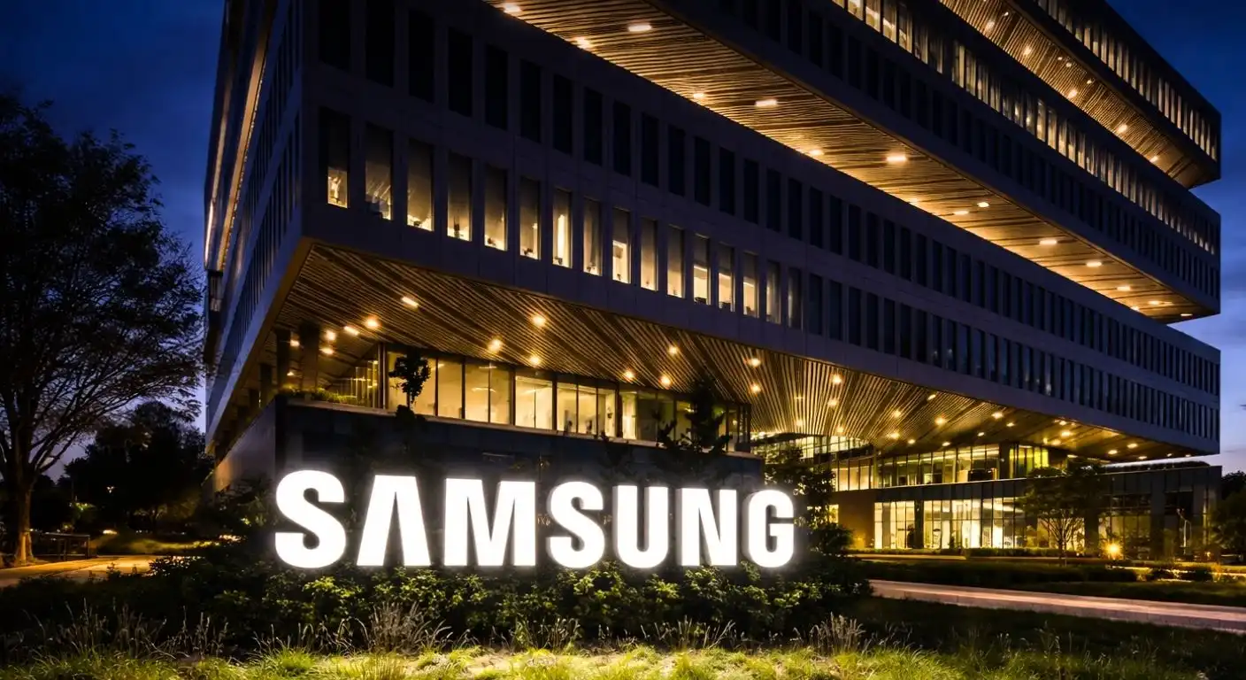
Samsung Electronics decided to aggressively speed up the launch of its massive semiconductor fabrication plant in Yongin, South Korea. Originally slated for completion in 2030, the technology giant now targets 2029 to bring the first advanced manufacturing line online. This schedule adjustment reflects a brutal reality in the global technology sector: artificial intelligence applications consume computing power at a rate that existing supply chains simply cannot sustain. To meet this skyrocketing demand and defend its market position against fierce international rivals, Samsung must bring new silicon manufacturing capacity to the market faster than ever before.
The Yongin facility represents the crown jewel of South Korea’s ambition to build the world’s largest semiconductor mega-cluster. Samsung committed an astonishing 300 trillion won, or roughly $230 billion, to develop this specific site over the next two decades. By pulling the operational date forward by an entire year, corporate leadership sent a clear signal to investors and competitors. The company refuses to lose ground in the race to manufacture the most advanced logic processors and high-capacity memory chips required by the artificial intelligence industry.
Building a semiconductor fabrication plant requires immense capital, pinpoint engineering, and massive logistical coordination. Shrinking a construction timeline of this magnitude forces the company to overhaul its engineering schedules, secure heavy construction materials early, and negotiate aggressive supply contracts for specialized lithography tools. The decision underscores the high stakes of the current semiconductor cycle, where a single year of delayed capacity can cost a company billions of dollars in lost contracts and permanently damage its relationship with top-tier technology clients.
The Strategic Shift Behind the Yongin Acceleration
The Yongin project spans an enormous 7.1 million square meters. Samsung plans to build five separate advanced fabrication facilities on this plot, surrounded by a supporting ecosystem of more than 150 domestic and international materials, parts, and equipment suppliers. Moving the first factory’s start date to 2029 requires an immediate mobilization of capital and labor.
Company executives recognize that the artificial intelligence hardware boom is not a temporary spike but a fundamental restructuring of global computing architecture. Tech companies no longer buy traditional server processors at the same volume; instead, they pour hundreds of billions of dollars into specialized accelerators and massive memory arrays. Samsung expects the Yongin hub to serve as its primary base for mass-producing sub-2-nanometer logic chips and next-generation memory products tailored specifically for these heavy data center workloads.
Government Infrastructure and Fast-Track Permitting
A project of this scale cannot advance without intense cooperation from the state. The South Korean government views the Yongin cluster as a matter of absolute national security and economic survival. To facilitate Samsung’s accelerated 2029 timeline, state agencies agreed to slash bureaucratic red tape and fast-track environmental and construction permits.
More importantly, the government promised to solve the two biggest bottlenecks in semiconductor manufacturing: electricity and water. Advanced chip factories consume mind-boggling amounts of resources. Estimates suggest the completed Yongin cluster will require more than 10 gigawatts of steady electrical power and upwards of 650,000 tons of ultrapure water every single day.
To meet the new 2029 deadline, the state-run Korea Electric Power Corporation is rushing to establish dedicated liquefied natural gas power plants to provide initial electricity, with plans to route power from distant nuclear and renewable sources through new transmission grids later. Similarly, water authorities are expediting the construction of massive pipeline networks to pull water from nearby reservoirs. Without this aggressive government intervention, Samsung could never compress a multi-billion-dollar construction schedule by an entire year.
Chasing TSMC in the Advanced Foundry Market
The accelerated timeline traces directly back to Samsung’s fierce rivalry with Taiwan Semiconductor Manufacturing Company. TSMC currently dominates the global foundry market, holding a market share that frequently exceeds 60%. Meanwhile, Samsung hovers between 11% and 13% in the contract manufacturing space.
TSMC secured the vast majority of the highly lucrative orders from companies like Nvidia, Apple, and Advanced Micro Devices. To break this monopoly, Samsung must offer clients comparable or superior manufacturing technology paired with massive, reliable production volume. The company expects its 2-nanometer and 1.4-nanometer manufacturing nodes to mature right as the first Yongin plant opens its doors.
If Samsung can successfully ramp up 2-nanometer yields by 2029 in a brand-new facility, it can offer global tech giants a viable, high-volume alternative to TSMC. Tech companies desperately want a second major supplier to reduce their reliance on Taiwan and negotiate better pricing. Samsung needs the Yongin capacity online and ready to accept these massive orders before TSMC locks clients into long-term contracts for the next decade of silicon architecture.
Competing in the High-Stakes AI Hardware Race
The generative artificial intelligence revolution changed the physics and economics of the semiconductor industry. Training large language models requires thousands of specialized graphics processing units working in perfect synchronization. These processors generate immense heat and require unprecedented data transfer speeds. To feed data to the processors fast enough, the industry relies on a specific technology that Samsung is heavily prioritizing.
The Exploding High-Bandwidth Memory Market
High-Bandwidth Memory determines the speed and efficiency of modern artificial intelligence accelerators. By stacking multiple memory chips vertically and connecting them with microscopic copper pillars called through-silicon vias, manufacturers create memory blocks that transfer data at blistering speeds while consuming very little physical space.
SK Hynix, a domestic rival, captured the early lead in this market by securing exclusive supplier agreements with Nvidia for early generations of High-Bandwidth Memory. Samsung spent the last two years aggressively trying to close this gap. The company developed 12-layer memory stacks and invested heavily in thermal compression bonding techniques to improve production yields.
Market analysts project the High-Bandwidth Memory market will grow from roughly $4 billion in 2023 to more than $20 billion in the coming years. By 2029, the industry will likely transition to sixth or seventh-generation memory stacks. These future generations will require advanced logic processors to serve as the base layer of the memory stack. Samsung’s new Yongin factory will possess the exact extreme ultraviolet lithography tools needed to print these complex base layers at a massive scale, allowing the company to capture a larger share of this explosive market.
Redefining Custom Silicon and Turnkey Solutions
Another massive trend driving Samsung’s urgency is the rise of custom silicon. Technology giants like Google, Amazon, Meta, and Microsoft realized that buying off-the-shelf accelerators costs too much and limits their ability to optimize their specific software models. Consequently, these companies formed massive internal engineering teams to design their own proprietary chips.
These technology giants design the architecture, but they need a physical factory to print the silicon, manufacture the memory, and package the disparate pieces together into a single component. Samsung is the only company in the world that possesses top-tier capabilities in all three of these areas: logic foundry, memory manufacturing, and advanced 2.5D and 3D packaging.
Samsung pitches this capability as a “turnkey solution.” Instead of a tech giant buying memory from SK Hynix, hiring TSMC to print the logic chip, and paying a third-party firm to package them together, they can hand the entire process to Samsung. Pushing the Yongin factory launch to 2029 allows Samsung to scale this turnkey service rapidly. The new facility will integrate seamlessly with Samsung’s existing memory campuses in Pyeongtaek and Hwaseong, creating an unparalleled geographic cluster that can handle a custom chip order from raw silicon design to final packaged delivery in record time.
The Geopolitical Push for Semiconductor Sovereignty
Global politics heavily influence corporate construction schedules. The semiconductor supply chain became the primary battleground in the ongoing technological conflict between the United States and China. Both superpowers recognize that whoever controls the supply of advanced silicon controls the future of military intelligence, economic productivity, and global communication networks.
The United States passed the CHIPS and Science Act, releasing $52 billion in subsidies to entice companies to build factories on American soil. Europe responded with a similar $47 billion legislative package. Japan also announced massive subsidies to revitalize its legacy chip industry. This global subsidy war threatens to pull manufacturing capability away from South Korea.
To defend its economic lifeblood, South Korea implemented the “K-Chips Act,” which expanded tax credits for large corporations investing in domestic semiconductor facilities from 8% to 15%, with additional incentives pushing the effective rate as high as 25%. Samsung’s decision to pour $230 billion into Yongin and speed up the timeline represents a direct response to this domestic policy support.
Strengthening the Domestic Silicon Shield
South Korea relies on the semiconductor industry for approximately 20% of its total export economy. The government and corporate leaders view domestic chip factories as a “silicon shield” that guarantees international diplomatic relevance and military security.
By building the world’s largest mega-cluster inside its own borders, South Korea ensures that the United States and other Western allies maintain a vested interest in the defense and stability of the Korean peninsula. However, international clients worry about geographic concentration risks. They fear that a localized natural disaster or regional conflict could wipe out their supply chain.
Samsung counters this fear by building facilities abroad, including a major new foundry in Taylor, Texas. Yet, the company reserves its most advanced research and high-volume bleeding-edge manufacturing for its domestic hubs. Accelerating the Yongin plant proves that Samsung intends to keep its center of gravity firmly planted in South Korea. The facility will house equipment that costs upwards of $350 million per machine, operated by the highest concentration of doctoral-level materials scientists and electrical engineers in the country.
Economic Ripples Across the Korean Peninsula
The financial impact of a $230 billion investment spread over two decades fundamentally alters the local and national economy. Building a semiconductor mega-cluster creates an economic gravity well that pulls in capital, specialized labor, and physical infrastructure.
When Samsung breaks ground on the accelerated 2029 factory, it will unleash billions of dollars into the local construction industry. Tens of thousands of construction workers, pipefitters, and heavy equipment operators will spend years building the reinforced concrete structures and specialized cleanrooms required to house vibration-sensitive lithography tools.
Once operational, the cluster will trigger a massive wave of indirect job creation. The South Korean government estimates that the Yongin semiconductor hub will generate 1.6 million direct and indirect jobs over its lifespan. The 150 companies planning to set up shop around the Samsung facility will hire thousands of software developers, chemical engineers, and logistics experts.
This clustering effect mirrors the success of Silicon Valley or Taiwan’s Hsinchu Science Park. When fabless design firms sit physically adjacent to the factory that prints their chips, they can resolve engineering defects faster and accelerate their product iteration cycles. Samsung wants to foster this tight-knit ecosystem to create a domestic talent pool that rivals any engineering hub on earth.
By pulling the factory launch forward to 2029, Samsung accelerates this entire economic timeline. Regional municipalities are already rewriting their urban development plans to accommodate the influx of high-income tech workers. They are building new housing developments, expanding public transportation lines, and opening new schools to support the families that will inevitably migrate to the Yongin area.
Samsung faces an incredibly narrow window to capitalize on the current artificial intelligence supercycle. The company understands that moving from a 2030 target to a 2029 operational launch requires taking on massive operational risk and spending capital at an uncomfortable velocity. However, the alternative—falling permanently behind TSMC in the foundry race or losing the memory crown to SK Hynix—presents a far greater threat to the company’s survival.
The next few years will test Samsung’s ability to execute complex heavy engineering while simultaneously advancing sub-2-nanometer physics in the laboratory. If the company successfully brings the Yongin mega-factory online by 2029, it will secure the production volume and technological edge necessary to supply the next generation of artificial intelligence data centers, cementing its status as the foundational pillar of the global digital economy.