

Key Points:
- Micron Technology announced the establishment of Micron Research Labs, backed by a planned $10 billion investment over the next decade.
- Headquartered on its Boise, Idaho campus, the facility marks the first dedicated long-horizon memory research hub in the United States.
- The center will focus on next-generation memory architectures, advanced silicon packaging, and future semiconductor manufacturing.
- The $10 billion research initiative builds upon Micron’s broader $250 billion domestic manufacturing and innovation commitments.
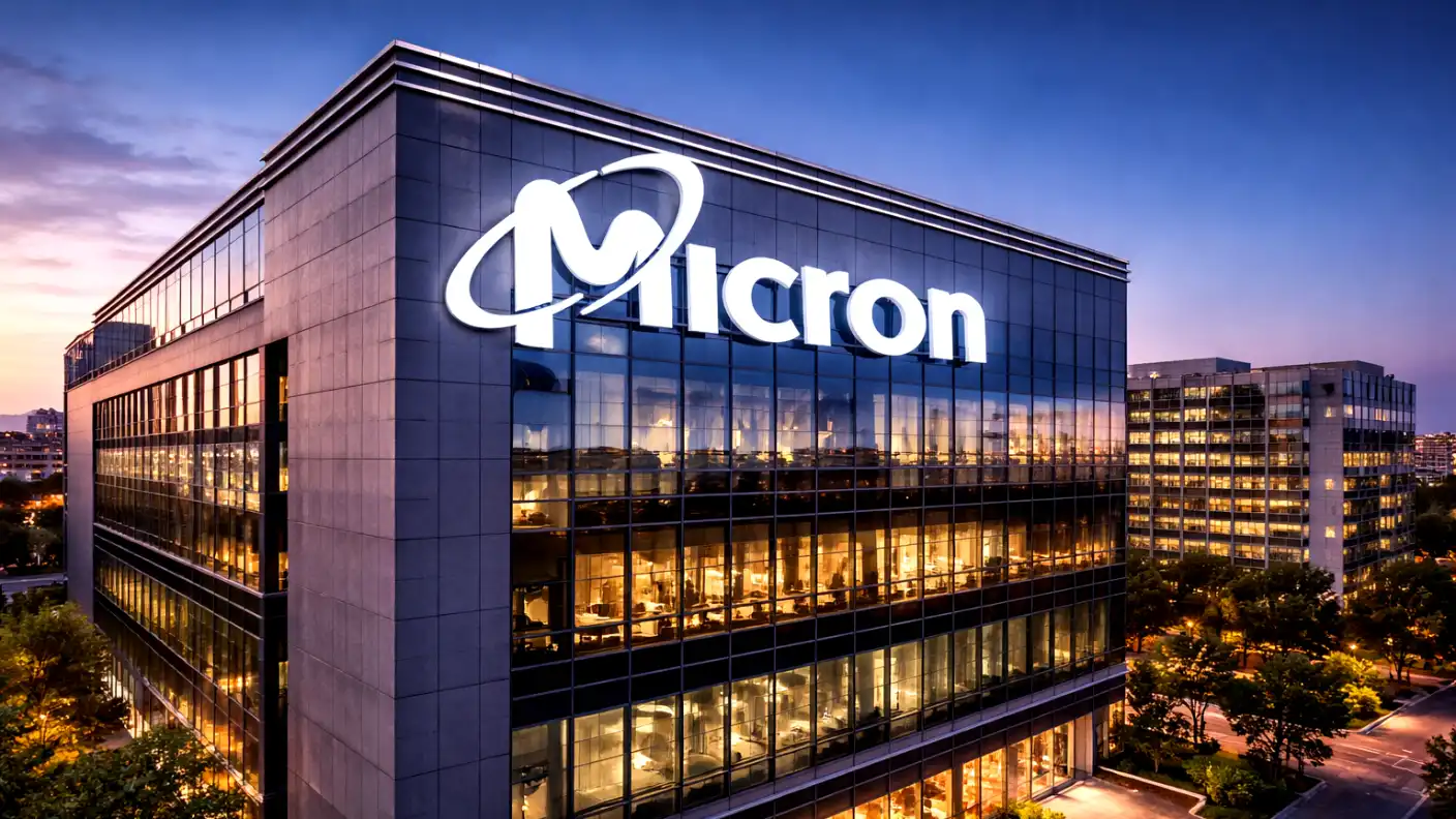
American semiconductor manufacturer Micron Technology has unveiled a landmark initiative to anchor future computing breakthroughs on domestic soil. The company officially introduced Micron Research Labs, a premier long-horizon research institution headquartered on its corporate campus in Boise, Idaho. Backed by a planned $10 billion investment over the next decade, the hub establishes the first dedicated semiconductor memory research institution of its kind in the United States.
The new institution will focus on exploring computing concepts that sit far beyond current industrial technology roadmaps. Engineering teams will concentrate on four foundational pillars: critical memory technologies, advanced memory-centric compute architectures, next-generation 3D packaging innovations, and future semiconductor manufacturing methodologies. By investigating novel materials and device physics ten to twenty years ahead of commercial lifecycles, the facility aims to eliminate the memory bottlenecks that threaten to constrain future artificial intelligence development.
Micron Research Labs is designed as an open, collaborative ecosystem bringing together industry partners, universities, national research laboratories, government agencies, and tech startups. The planned $10 billion capital deployment will fund direct research chairs, extensive university fellowship programs, and global satellite research hubs connected to facilities in Europe, Japan, India, Singapore, and Taiwan. Technology industry leaders from major hardware giants—including Nvidia, Apple, Applied Materials, and Lam Research—expressed strong support for the unified research network.
Construction on the flagship Boise research campus is scheduled to break ground in 2027. The state-of-the-art facility will feature advanced laboratory cleanrooms capable of hosting hundreds of specialized semiconductor physicists, materials scientists, and software engineers. Furthermore, the campus will house specialized event facilities to host international technology symposiums, research forums, and collaborative engineering workshops.
A major strategic advantage of the Boise site is its direct co-location with Micron’s expanding high-volume manufacturing fabs. The company is currently constructing two mega-fabs, known as ID1 and ID2, adjacent to its existing 250,000-square-foot research cleanroom in Boise. Co-locating long-horizon research alongside active fabrication lines allows scientists to rapidly transfer experimental discoveries directly into high-volume production, significantly shortening the time required to commercialize advanced High Bandwidth Memory and next-generation dynamic random-access memory chips.
The $10 billion research initiative operates separately from and builds upon the more than $250 billion that Micron has committed to manufacturing and advanced research across the United States. In addition to the multi-billion-dollar Boise expansion, the chipmaker is advancing a massive mega-fab complex in Central New York, modernizing its automotive and industrial memory facility in Virginia, and expanding domestic advanced packaging lines. Supported by federal and state manufacturing incentives, the comprehensive strategy aims to produce 40% of the company’s leading-edge DRAM output within the United States by 2035.
The massive capital commitment arrives as the global technology sector recognizes that memory performance dictates the ceiling of artificial intelligence capabilities. While high-performance graphics processing units handle mathematical computations, training and operating massive multimodal models require moving terabytes of data every millisecond between processors and memory arrays. Chief Executive Officer Sanjay Mehrotra emphasized that the decisions made today will determine who leads tomorrow’s digital economy, asserting that America’s artificial intelligence future must rely on domestically developed and manufactured memory systems.
Federal officials highlighted the national security importance of securing domestic leadership in memory development. For decades, advanced memory fabrication and packaging concentrated heavily in East Asia, leaving Western technology supply chains vulnerable to geopolitical instability and maritime shipping chokepoints. Establishing a premier domestic research hub ensures that critical intellectual property, proprietary tooling, and advanced packaging techniques remain anchored within the United States.
As the global semiconductor industry races toward smaller process nodes and complex 3D architectures, foundational research serves as the ultimate competitive moat. By committing $10 billion to build Micron Research Labs in Boise, the company is ensuring that American engineers continue defining the future of memory technology. The long-term initiative provides the physical infrastructure, funding, and talent pipeline necessary to power the next century of computing innovation.