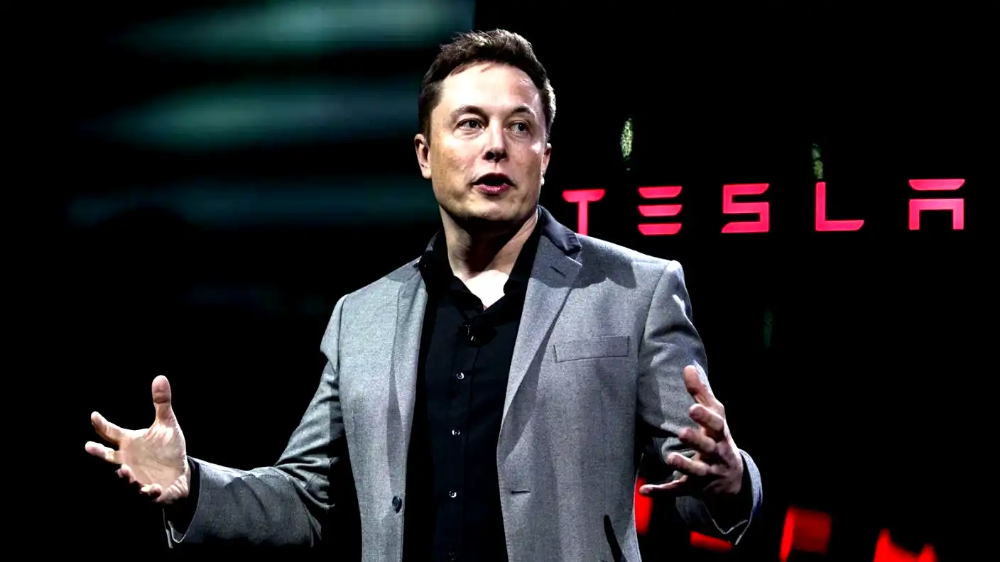
Tesla and SpaceX have joined forces to launch one of the most ambitious manufacturing projects in industrial history. The two tech giants are developing a mega-scale semiconductor fabrication complex known as Terafab. Located in Grimes County, Texas, northwest of Houston, this landmark initiative seeks to solve the growing silicon bottleneck that threatens the future of robotics, artificial intelligence, autonomous transport, and commercial space exploration.
The project represents a joint financial commitment that starts with an initial phase valued at $16.8 billion and could scale to a total investment of $119 billion across multiple buildout phases. With a planned footprint exceeding 100 million square feet under a single contiguous roof, Terafab aims to surpass every existing industrial complex on Earth. The facility will combine raw silicon processing, advanced logic fabrication, memory production, packaging, and testing into one unified pipeline.
The industrial world is racing to secure artificial intelligence hardware, but external chip supply chains face tight capacity limits and geopolitical vulnerabilities. By designing, manufacturing, and packaging silicon in-house, Tesla and SpaceX intend to generate more than 1 terawatt of dedicated computing capacity every single year. This vertical integration strategy will fundamentally reshape how both enterprises scale their next-generation technologies.
A Colossal Vision for American Semiconductor Independence
Modern technology companies usually rely on third-party foundries spread across Asia and North America to build microchips. While fabless chipmakers design brilliant silicon architectures, they remain vulnerable to wafer shortages, logistical delays, and assembly backlogs. Terafab breaks away from this traditional outsourced model by establishing full domestic sovereignty over the silicon lifecycle.
Tesla and SpaceX require custom compute solutions tailored strictly to real-time physical workloads. Autonomous vehicles making split-second decisions cannot rely on generic server chips. Similarly, humanoid robots operating in unstructured human environments demand low-latency edge silicon with extreme energy efficiency. SpaceX vehicles, deep-space communication nodes, and orbital satellite constellations demand radiation-hardened components built to survive extreme temperatures. Bringing these distinct semiconductor requirements under one corporate umbrella allows both companies to customize wafer parameters and accelerate product iterations without waiting in line at commercial foundries.
The sheer scale of the investment demonstrates that custom silicon has become the single most vital raw material for modern automation. Building a dedicated manufacturing base in Texas guarantees continuous hardware flow for both consumer vehicles and interplanetary spacecraft.
Breaking Architectural Records with 100 Million Square Feet
The planned dimensions of Terafab challenge conventional engineering standards. The facility will cover more than 100 million square feet of floor area, making it roughly 35 million square feet larger than the current record-holder, the AvtoVAZ automotive plant in Russia, which spans 65 million square feet. For comparison, the entire structure will contain approximately 10 times the usable floor area of Giga Texas in Austin.
Architectural plans reveal a symmetrical layout featuring dual manufacturing wings connected by a central logistics highway and cleanroom corridor. The building envelope utilizes specialized vibration-dampening foundations sunk deep into the Texas bedrock. Extreme lithography processes require absolute mechanical stability, because even microscopic vibrations from nearby highways or heavy equipment can ruin silicon wafers etched at nanometer scales.
Integrating raw material delivery docks, chemical storage, cleanroom suites, sub-fab utility basements, and automated post-packaging facilities into a single building eliminates the logistical lag that plagues standard chip manufacturing. Traditional chips often travel across three continents before reaching a circuit board. Terafab keeps every step within a single climate-controlled ecosystem.
Unpacking the $119 Billion Multi-Phase Capital Strategy
Developing a cleanroom facility of this magnitude demands massive capital deployment. The joint venture allocates $16.8 billion to the initial development phase, covering site preparation, foundation construction, utility substation infrastructure, and cleanroom installations.
As cleanroom modules reach operational status, the total investment across subsequent expansion phases will reach an estimated $119 billion. Advanced extreme ultraviolet lithography machines, high-purity chemical distribution networks, and automated wafer transport vehicles account for more than 60% of the long-term budget. Tesla and SpaceX are pooling balance sheet reserves, private funding allocations, and commercial cash flows to finance the project.
This capital strategy balances immediate near-term production goals with decade-long expansion plans. By investing in scalable modular architecture, the site can start fabricating initial prototype silicon wafers while construction crews erect adjacent wings. This phased deployment protects the joint venture from sudden macroeconomic shifts while delivering silicon to operational assembly lines as fast as possible.
The Compute Crisis Driving In-House Silicon Fabrication
Artificial intelligence development has transitioned from a software challenge to a raw hardware bottleneck. The global supply of high-end graphics processors and custom accelerators remains deeply constrained. Wait times for cutting-edge wafers stretch past 12 months at major foundries, and rising packaging costs continue to squeeze margins across the hardware sector.
Elon Musk and executive teams at both companies realized that relying solely on outside merchant silicon vendors places a strict ceiling on corporate growth. If Tesla intends to manufacture millions of autonomous vehicles and millions of humanoid robots annually, the company needs a silicon supply chain that exceeds total global output today.
Terafab is engineered specifically to produce 1 terawatt of aggregate compute power annually. This volume of operational processing power will satisfy the internal roadmaps of both companies while insulating them from external market shortages.
Meeting the Exponential Appetite of Optimus and Autonomous Fleets
Tesla allocates roughly 25% of Terafab’s planned annual compute output directly to its terrestrial robotics and automotive divisions. The rapid expansion of the Full Self-Driving software suite and the commercial rollout of driverless Cybercab fleets demand continuous hardware upgrades.
Autonomous vehicles depend on high-efficiency onboard neural processing units capable of processing high-definition camera streams in fractions of a millisecond. A commercial fleet numbering tens of millions of vehicles requires a reliable pipeline of millions of automotive-grade processors every quarter.
The compute demands of the Optimus humanoid robot project are even larger. Unlike a vehicle that moves primarily along paved two-dimensional roads, a humanoid robot must navigate complex physical spaces, manipulate delicate objects, and process real-time tactile feedback. Optimus requires dual onboard compute units for motor control and visual understanding, as well as vast centralized supercomputing clusters to train foundation behavior models. Terafab will supply both the low-power chips running inside the robot bodies and the enterprise chips running in backend training clusters.
Powering SpaceX Spacecraft and Orbital AI Data Clusters
SpaceX claims the remaining 75% of Terafab’s silicon production capacity to fuel its aerospace initiatives and space-based compute clusters. Modern spacecraft engineering relies heavily on real-time sensor processing, autonomous orbital navigation, and high-frequency communication relays.
The Starship launch vehicle program requires advanced microcontrollers and telemetry processors that withstand high g-forces, sonic vibration, and severe thermal cycles during atmospheric reentry. Terafab will manufacture ruggedized silicon components built from custom alloys and specialized substrate layers.
SpaceX also plans to deploy massive orbital computing systems, known as Starmind constellations. These networks of satellite data centers will process telemetry, space observation data, and terrestrial cloud computing tasks directly in low Earth orbit. Operating data centers in orbit requires radiation-hardened microchips that manage heat through radiative cooling rather than airflow. Producing these specialized processors in-house gives SpaceX full control over space-grade silicon architecture.
Total Vertical Integration Under One Massive Roof
The modern semiconductor industry is notoriously fragmented. A standard microchip is designed in California, etched on silicon wafers in Taiwan, shipped to Malaysia for packaging, transported to Vietnam for board testing, and finally flown to assembly plants in North America or Europe. This distributed supply chain creates dozens of single-point vulnerabilities.
Terafab eliminates the geographic friction of the semiconductor supply chain by establishing a completely integrated production loop inside Grimes County. Every step from raw wafer input to completed, tested compute module happens inside the same building complex.
Combining Logic, Memory, Advanced Packaging, and Testing
Vertical integration at Terafab goes far beyond silicon wafer etching. Modern high-performance artificial intelligence chips rely heavily on advanced 3D packaging, where compute logic dies sit directly atop high-bandwidth memory stacks using microscopic through-silicon vias.
Separating logic manufacturing from memory fabrication introduces massive logistics delays and yield losses. Terafab solves this by combining the following five core manufacturing disciplines within one continuous facility:
- Silicon wafer fabrication and extreme ultraviolet lithography processing.
- High-bandwidth memory module synthesis and high-density storage manufacturing.
- Advanced 2.5D and 3D heterogeneous multi-chip packaging.
- Automated thermal interface application and substrate mounting.
- High-throughput automated diagnostic testing and environmental stress screening.
Housing these five processes under one roof cuts production cycle times from months down to days. Engineers can spot design defects during wafer fabrication, adjust the lithography masks immediately, and verify the fix in packaged modules within the same week. This rapid feedback loop gives Tesla and SpaceX an immense development advantage over competitors who wait months for revised wafers from overseas partners.
Relieving Pressure on Global Chip Foundries
While Tesla and SpaceX maintain active business relationships with leading merchant foundries, their internal chip demands threaten to overwhelm commercial capacity. By shifting high-volume internal designs to Terafab, both companies free up capacity at external suppliers while insulating themselves from price swings.
Global foundry utilization rates frequently exceed 90%, causing severe price volatility during consumer electronics upgrade cycles. When smartphone and personal computer makers rush to book cleanroom capacity, automotive and aerospace companies often face extended delivery delays.
Terafab removes this dependency entirely. The facility functions as an internal utility for Tesla and SpaceX, prioritizing production based on internal vehicle and rocket manufacturing schedules rather than open-market auction pricing. This structure delivers predictable component costs and eliminates unexpected production shutdowns caused by third-party chip allocations.
Economic Impacts and Regional Transformation in Texas
The construction of Terafab accelerates the ongoing transformation of Texas into a premier global semiconductor hub. The state has already attracted tens of billions of dollars in private technology infrastructure, and this joint venture cements that leadership position.
Grimes County offers the geographical space, access to major transportation corridors, and proximity to regional engineering hubs needed for a project of this scale. The development will bring profound economic benefits to surrounding communities while requiring unprecedented investments in civil infrastructure.
Workforce Expansion and High-Tech Job Creation in Grimes County
The initial development phase of Terafab will create roughly 3,000 direct, permanent high-tech jobs on-site. These roles range from cleanroom technicians and process engineers to material scientists, software developers, and facility maintenance experts.
Secondary employment effects will generate thousands of additional jobs across regional supply chains. Equipment suppliers, industrial chemical producers, specialty gas distributors, and logistics firms will expand local operations to serve the megafactory.
Tesla and SpaceX plan to partner with Texas universities and regional technical colleges to build workforce training pipelines. Specialized apprenticeship programs will train technicians in cleanroom protocols, advanced vacuum system maintenance, and precision robotics operation. This investment in human capital ensures a steady stream of local technical talent capable of operating complex semiconductor fabrication tools.
Energy Demands and Sustainable Infrastructure Challenges
Operating a semiconductor factory spanning 100 million square feet requires staggering amounts of electrical power, cooling capacity, and ultra-pure water. Semiconductor fabs are energy-intensive facilities that run sensitive machinery 24 hours a day, 365 days a year without interruption.
Terafab’s power strategy incorporates large-scale on-site renewable energy generation, massive stationary battery energy storage systems, and dedicated grid substations. The facility will integrate solar panel arrays across its expansive curving roof and utilize Megapack battery installations to provide uninterrupted power during grid fluctuations.
Water stewardship represents another critical design pillar. Advanced chip fabrication requires millions of gallons of ultra-pure water daily to clean silicon wafers between lithography and etching steps. Terafab integrates an industrial closed-loop water reclamation plant designed to recycle more than 98% of all process water. On-site wastewater treatment facilities will purify used chemicals and industrial runoff, minimizing the complex’s impact on local water tables.
Strategic Implications for the Global Tech Ecosystem
The creation of Terafab signals a structural shift in how modern industrial conglomerates approach high technology. Software capabilities alone are no longer enough to maintain an industry lead. The physical hardware running the code determines the ultimate ceiling of any artificial intelligence enterprise.
Controlling the hardware stack from the raw atomic level up to the cloud software layer gives Tesla and SpaceX unprecedented agility. This integrated operational philosophy mirrors early industrial empires while leveraging the most advanced manufacturing science of the modern era.
Supply Chain Sovereignty in an Unstable Global Market
Geopolitical tensions, trade disputes, and natural disasters present constant hazards to international semiconductor supply chains. Over 80% of the world’s most advanced logic chips currently originate in a concentrated geographic area in East Asia. A disruption in regional shipping routes or unexpected factory shutdowns could freeze global manufacturing across the automotive, robotics, and aerospace sectors.
Terafab establishes a fully domestic supply chain capable of producing advanced silicon entirely on American soil. By controlling intellectual property, fabrication tooling, chemical sourcing, and packaging facilities inside the United States, Tesla and SpaceX protect their strategic roadmaps from foreign trade barriers and logistical gridlock.
This sovereignty extends beyond physical security. It also shields proprietary chip architectures from industrial espionage and unauthorized cloning. Custom neural accelerators and space-grade control circuits remain protected within private internal facilities throughout their entire operational life.
The Long-Term Road to Terawatt-Scale AI Hardware
Scaling artificial intelligence hardware to the terawatt level marks the frontier of computing science. A terawatt represents one trillion watts of continuous operational computing capacity, a figure that dwarfs the current aggregate deployment of all global artificial intelligence data centers combined.
Reaching this milestone requires rethinking every layer of the compute stack, including the following crucial engineering domains:
- Sub-nanometer transistor architectures that reduce parasitic capacitance and leakage current.
- Heterogeneous chip integration combining optical interconnects directly on the silicon die.
- Direct-to-chip liquid cooling systems capable of dissipating high thermal design power.
- Highly resilient, fault-tolerant circuit design to maintain uptime in extreme operating environments.
Terafab serves as the dedicated engine to realize this terawatt-scale vision. By iterating silicon designs rapidly under the same roof where technicians test and assemble finished products, Tesla and SpaceX will accelerate the development cycle of advanced computing hardware.
The joint venture between Tesla and SpaceX to build the Terafab complex in Grimes County, Texas, represents far more than an ordinary factory construction project. It stands as an audacious restructuring of the global high-tech supply chain. By investing up to $119 billion into a 100-million-square-foot megafactory, the two companies are taking decisive control over their technological destinies. As artificial intelligence, autonomous transport, robotics, and commercial spaceflight converge, Terafab will provide the raw silicon horsepower needed to drive the next century of industrial automation.