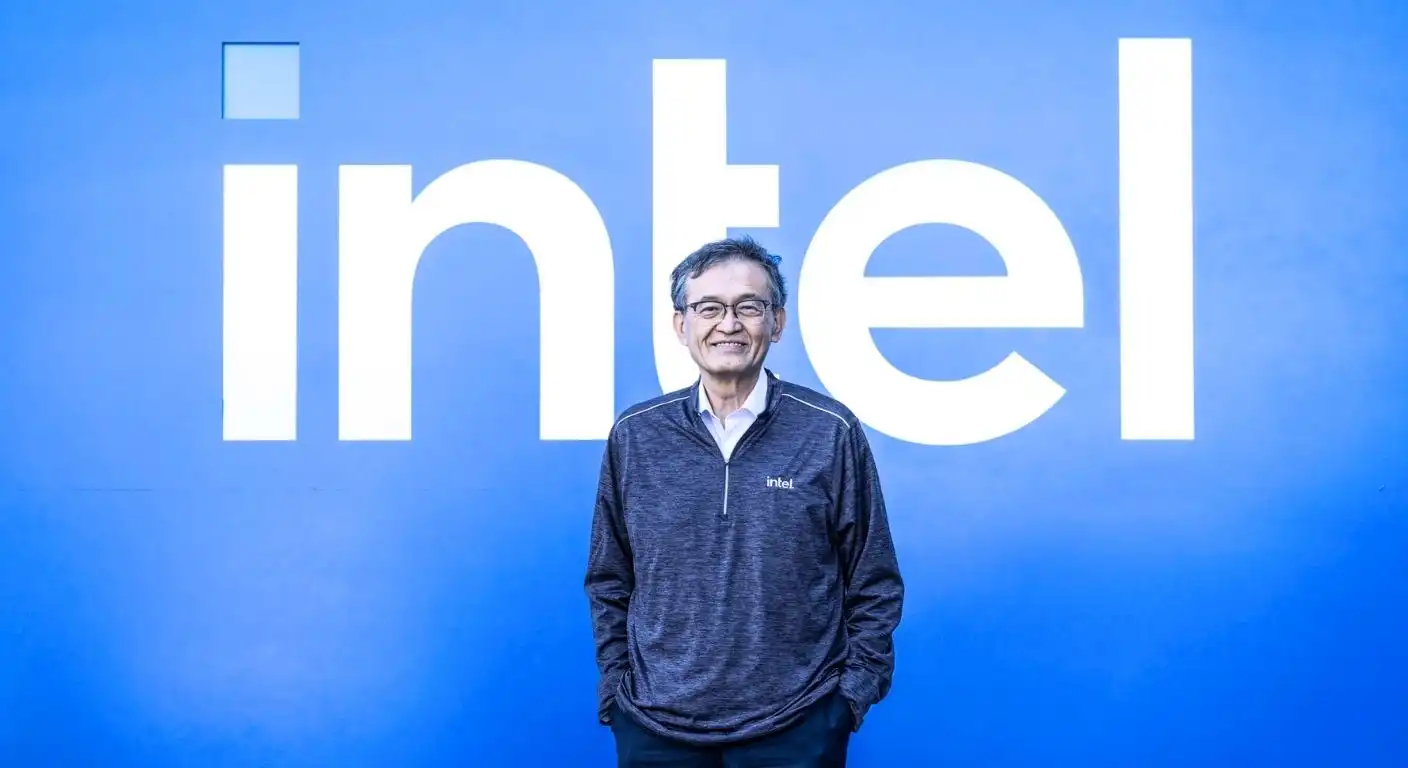
In an unprecedented departure from its historical corporate strategy, Intel Corporation signed a major intellectual property licensing and manufacturing agreement with a new artificial intelligence semiconductor startup co-founded and led by veteran chip investor Lip-Bu Tan. Under the terms of the strategic deal, Intel will supply proprietary microprocessor technology, specialized interconnect designs, and priority manufacturing access on its flagship Intel 18A process node. The rare technology transfer allows the newly formed startup to build custom artificial intelligence chiplets that integrate natively with Intel’s x86 ecosystem.
The transaction marks a significant moment in the semiconductor industry. For decades, Intel guarded its x86 instruction set architecture and advanced manufacturing processes with fierce legal protection, using them exclusively to produce its own internal processors. By licensing proprietary x86 intellectual property and providing commercial foundry services to an external startup, Intel is demonstrating a fundamental shift toward an open foundry model. The strategy aims to prove to global fabless chip designers that Intel Foundry Services can successfully manufacture complex, customized silicon architectures.
The deal also carries significant personal and corporate history. Lip-Bu Tan, a respected semiconductor venture capitalist and former Chief Executive Officer of Electronic Design Automation giant Cadence Design Systems, previously served on Intel’s board of directors. Tan resigned from Intel’s board following strategic disagreements over the pace of the company’s foundry turnaround and manufacturing execution. Re-engaging with Tan through a joint venture and technology licensing agreement signals that Intel leadership recognizes the value of Tan’s deep relationships across the global fabless startup community.
TechGolly provides a comprehensive technical and business analysis of Intel’s agreement with Lip-Bu Tan’s startup, evaluating x86 licensing mechanics, 18A process node physics, PowerVia backside power delivery, Foveros 3D packaging, foundry competition with TSMC, and the broader commercial outlook for custom AI accelerators.
Unpacking the Intel and Lip-Bu Tan Semiconductor Alliance
The strategic alliance between Intel and Lip-Bu Tan’s new startup establishes a fresh template for how established semiconductor giants can partner with emerging venture-backed chip designers. Under the terms of the agreement, Intel and Tan’s venture fund, Walden International, alongside a syndicate of private venture capital partners, are co-investing tens of millions of dollars in seed capital to fund the startup’s initial research and development pipeline.
In exchange for equity participation and long-term manufacturing commitments, Intel is providing the startup with direct access to a rich portfolio of intellectual property. The startup receives license rights to low-power x86 CPU cores, high-bandwidth memory interface blocks, and advanced die-to-die interconnect protocols. Access to this core IP allows the startup’s engineering team to avoid spending years designing basic computing blocks from scratch, focusing their engineering resources entirely on proprietary artificial intelligence acceleration units.
The primary product roadmap for the startup centers on designing custom, heterogeneous chiplets engineered specifically for high-throughput artificial intelligence inference in data centers and edge computing networks. By pairing low-latency x86 CPU cores directly with custom AI acceleration matrix engines on a single silicon substrate, the startup aims to deliver high-performance compute units that run standard enterprise software without requiring complex code translation layers.
Furthermore, the deal includes a binding commercial manufacturing agreement. The startup will fabricate its custom chips at Intel Foundry facilities using the advanced Intel 18A process node. Securing a high-profile, venture-backed customer for 18A provides Intel with a critical commercial showcase, demonstrating to the global technology market that its newest manufacturing node can meet the rigorous yield, performance, and defect-density standards required by independent chip designers.
The Lip-Bu Tan Factor: Cadence, Walden, and Semiconductor VC Power
To understand why Intel agreed to license its core technology to a new startup, industry analysts point directly to the immense reputation and market influence of Lip-Bu Tan.
Over a career spanning four decades, Lip-Bu Tan established himself as one of the most influential figures in the global semiconductor ecosystem. As Chief Executive Officer of Cadence Design Systems, he led a major corporate turnaround, building Cadence into a dominant provider of Electronic Design Automation software used by virtually every major chip designer in the world. As founder and chairman of Walden International, Tan pioneered venture capital investing in early-stage microelectronics, backing over 100 successful semiconductor startups across North America, Europe, and Asia.
When Tan joined Intel’s board of directors, corporate leadership hoped his deep technical expertise and relationships with fabless chip executives would accelerate the growth of Intel Foundry Services. Although Tan eventually resigned from the board due to frustration over internal bureaucracy and manufacturing execution delays, his professional relationship with Intel Chief Executive Officer Pat Gelsinger remained grounded in mutual respect.
By partnering with Tan on his new AI startup, Intel gains an invaluable advocate within the venture capital community. If Tan’s startup successfully fabricates high-performing, high-yield AI chips on Intel’s 18A node, it will provide a powerful proof-of-concept that encourages other venture-backed chip startups to choose Intel Foundry over traditional Asian foundries.
The Technical Breakthrough: Intel 18A Process Node and PowerVia Architecture
The technological cornerstone of the deal is Intel’s 18A process node, which represents the company’s 1.8-nanometer-class semiconductor manufacturing technology. Intel 18A is the culmination of the company’s aggressive strategy to execute five process nodes in four years, designed to surpass competing foundries in transistor density and power efficiency.
Intel 18A introduces two revolutionary physical manufacturing innovations that represent a major departure from legacy silicon manufacturing:
First, RibbonFET Gate-All-Around (GAA) transistor architecture. For over a decade, the semiconductor industry relied on FinFET 3D transistors, where a thin vertical fin of silicon is surrounded on three sides by a gate electrode. As transistor dimensions shrank below 3 nanometers, FinFETs suffered from electrical current leakage and performance degradation. RibbonFET replaces vertical fins with stacked horizontal silicon nanosheets surrounded by the gate electrode, providing total four-side electrical control over the channel, enabling faster transistor switching speeds and lower power leakage.
Second, PowerVia backside power delivery technology. In traditional semiconductor manufacturing, both signal-carrying wires and electrical power lines are woven together in a complex, multi-layer interconnect stack built on top of the silicon transistors. This traditional approach creates severe wiring congestion, where power lines crowd out signal wires and cause resistance-driven voltage drops that waste energy.
PowerVia solves this physical bottleneck by completely separating power delivery from signal routing. Intel’s manufacturing process builds the power grid on the backside of the silicon wafer, while constructing the signal interconnect layers exclusively on the front side. Nano-vias etch directly through the silicon substrate to deliver electrical power straight to the transistors from behind.
Moving power delivery to the backside delivers extraordinary physical performance gains:
- First, it eliminates signal wire congestion on the front side of the chip, allowing chip designers to pack transistors closer together and increase overall compute density.
- Second, it reduces internal resistance and voltage drop, enabling transistors to operate at 15% to 20% higher clock frequencies at equivalent power levels.
- Third, it improves thermal dissipation, allowing high-power artificial intelligence processors to operate continuously at peak performance without thermal throttling.
Advanced Packaging Synergy: Foveros 3D and Heterogeneous Chiplets
In addition to 18A front-end wafer fabrication, Tan’s startup will utilize Intel’s advanced Foveros 3D packaging technologies to assemble its final commercial chiplets.
Modern artificial intelligence processors are too large and complex to manufacture as a single, monolithic piece of silicon. Large monolithic chips suffer from low manufacturing yields, as a single microscopic defect can ruin an entire multi-thousand-dollar die. To solve this cost challenge, the industry has transitioned toward heterogeneous chiplet architectures, where larger processors are broken down into smaller, individual silicon tiles manufactured on optimal process nodes and bound together inside a single protective package.
Intel’s Foveros 3D packaging technology allows chip designers to stack logic tiles, memory blocks, and I/O controllers vertically on top of a base silicon interposer. Using high-density micro-bumps and Through-Silicon Vias (TSVs), Foveros enables thousands of high-speed, low-latency electrical connections between stacked tiles, allowing separate chiplets to communicate with the speed and efficiency of a single monolithic chip.
Utilizing Foveros 3D packaging allows Tan’s startup to construct modular AI processors. The engineering team can pair low-power x86 CPU tiles manufactured on Intel 18A with specialized AI matrix accelerator tiles and high-bandwidth memory (HBM3e/HBM4) stacks within a single compact package, creating a highly customized computing solution for high-density server racks.
IDM 2.0 Transformation: Proving Intel Foundry’s Commercial Viability
The technology deal with Lip-Bu Tan’s startup represents a vital validation milestone for Intel Chief Executive Officer Pat Gelsinger’s IDM 2.0 transformation strategy.
Under its historical Integrated Device Manufacturing (IDM) model, Intel functioned as a closed, vertically integrated enterprise. Intel designed its own microprocessors, manufactured them exclusively in its own factories, and sold them directly to computer manufacturers. However, as manufacturing costs escalated and competing fabless chipmakers like Nvidia, AMD, and Apple partnered with specialized foundries like TSMC, Intel lost its long-standing manufacturing technology lead.
Gelsinger’s IDM 2.0 strategy fundamentally restructured the company, splitting Intel into two distinct operating units: Intel Products, which designs chips, and Intel Foundry, an independent, commercial foundry business that manufactures chips for both internal Intel divisions and external fabless clients.
To achieve its corporate goal of becoming the world’s second-largest commercial foundry by 2030, Intel Foundry must win multi-billion-dollar manufacturing contracts from major external chip design firms. However, foreign fabless companies historically hesitated to commit their high-value chip designs to Intel, fearing that Intel might prioritize its own internal processor production or expose client intellectual property to internal competing design teams.
By establishing strict operational firewalls between its design and foundry divisions, and by signing a high-profile technology transfer agreement with a respected industry leader like Lip-Bu Tan, Intel is proving that its commercial foundry operations are transparent, independent, and open for business.
Winning Tan’s startup adds another high-profile customer to Intel Foundry’s growing 18A customer pipeline, which includes multi-billion-dollar commercial commitments from Microsoft for custom Azure server chips, Amazon Web Services for custom AI infrastructure, and the United States Department of Defense under the Secure Enclave national security chip program.
The AI Accelerator Market: Challenging Nvidia and Broadcom Dominance
The commercial market target for Tan’s new startup is the booming, multi-billion-dollar global artificial intelligence accelerator market, currently dominated by Nvidia’s graphics processing units and Broadcom’s custom ASIC division.
As technology hyperscalers, cloud providers, and enterprise corporations spend over $200 billion annually constructing artificial intelligence data centers, the cost of purchasing off-the-shelf commercial GPUs has become a major operational burden. Enterprise buyers are seeking specialized, cost-effective custom silicon designed specifically for AI inference—the daily operational process of running trained AI models to answer user queries, generate code, and process real-time data.
Custom AI inference workloads require high memory bandwidth and low latency rather than the massive, raw floating-point compute power needed for pre-training foundation models. By integrating licensed x86 CPU cores directly onto the same package as custom AI accelerator tiles, Tan’s startup aims to deliver inference chips that execute enterprise software logic and neural network matrix math on a single, highly efficient processor.
If the startup successfully delivers high-performance, low-power inference chiplets on Intel’s 18A node, it will capture a lucrative market niche among enterprise customers looking to deploy cost-effective, domain-specific AI automation across their corporate data center networks.
Strategic Outlook for the Global Semiconductor Ecosystem
The technology transfer agreement between Intel and Lip-Bu Tan’s startup marks a permanent shift toward a more open, collaborative, and geographically diversified global semiconductor ecosystem.
Looking forward through the late 2020s, the global chip industry is evolving away from rigid proprietary silos toward modular, open-architecture chiplet ecosystems. The combination of open instruction set choices, standardized advanced packaging interfaces, and independent commercial foundries allows small, venture-backed design teams to build high-performance silicon that previously required the resources of a multi-billion-dollar corporate giant.
For the United States semiconductor industry, the success of Intel 18A carries major geopolitical significance. Backed by tens of billions of dollars in federal grants and tax incentives under the CHIPS and Science Act, Intel’s manufacturing expansion in Oregon, Arizona, Ohio, and New Mexico is rebuilding leading-edge commercial semiconductor fabrication capacity on American soil.
Establishing a viable, leading-edge commercial foundry in North America reduces global technology reliance on Asian manufacturing hubs, creating a resilient, geographically secure supply chain for advanced artificial intelligence chips, military microelectronics, and critical national infrastructure components.
If Intel successfully executes its 18A manufacturing ramp and expands its IP licensing partnerships with independent design startups, it will establish a self-sustaining commercial ecosystem that fuels North American semiconductor innovation for decades to come.
Key Takeaways for Chip Designers, VCs, and Tech Executives
The landmark technology deal between Intel and Lip-Bu Tan’s AI startup delivers crucial strategic insights for semiconductor executives, fabless chip architects, venture capital partners, and corporate technology leaders.
First, open intellectual property licensing is essential for foundry scaling. Leading-edge foundries cannot rely solely on internal product lines; they must open their proprietary IP libraries and design rules to external partners to drive high-volume wafer production and maximize factory utilization rates.
Second, backside power delivery and gate-all-around architectures represent the new baseline for advanced silicon performance. Chip designers seeking maximum compute density and energy efficiency must build their next-generation product roadmaps around advanced manufacturing nodes like Intel 18A that feature PowerVia and RibbonFET technologies.
Third, custom chiplets offer the fastest path to artificial intelligence monetization. Enterprise technology buyers are demanding specialized, cost-effective inference accelerators tailored to specific software workloads, creating massive commercial opportunities for nimble, venture-backed chiplet design startups.
Finally, commercial execution and trust dictate foundry leadership. By pairing leading-edge process engineering with transparent corporate governance and respected industry leadership, semiconductor foundries can earn global market trust, win high-value commercial design contracts, and shape the physical computing foundation of the digital future.