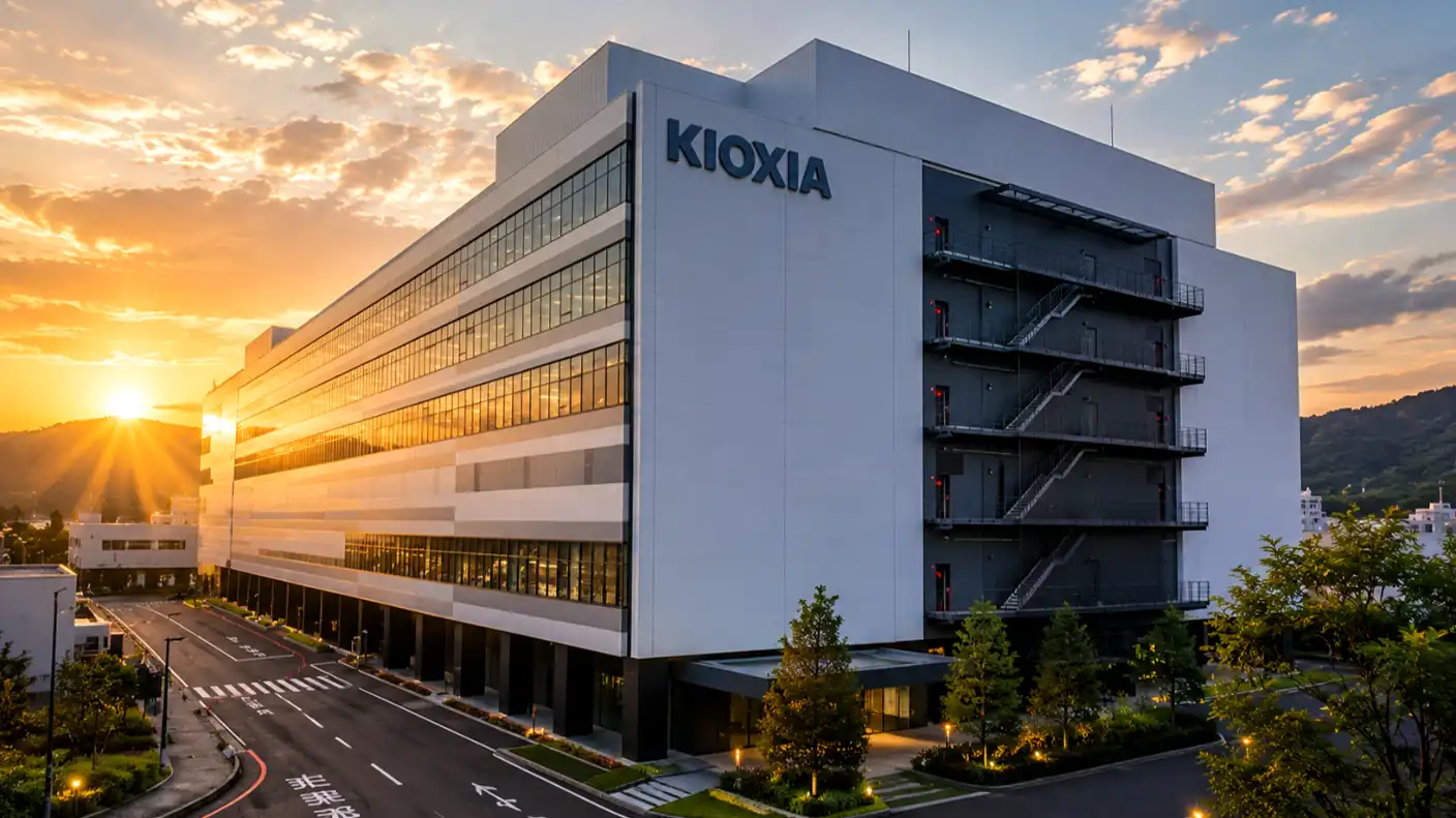
The physical infrastructure supporting the global artificial intelligence boom is entering a highly intensive phase of technological innovation. In August 2026, memory industry leaders Kioxia Corporation and SanDisk Corporation, a subsidiary of Western Digital, jointly announced the official launch of their ninth-generation 2-terabit Quad-Level Cell 3D flash memory technology. This advanced memory platform is engineered specifically to meet the rapidly expanding storage and processing demands of global AI-driven infrastructure and cloud data centers.
The release represents a major technological milestone, introducing unprecedented interface speeds and power efficiencies to the non-volatile memory market. As companies around the world pour billions of dollars into constructing massive, high-density server farms to train and run generative AI models, they require a new class of solid-state storage that can read and write vast data sets with minimal latency. The ninth-generation QLC technology addresses this need, delivering a massive performance upgrade over previous generations.
This latest product launch highlights the ongoing strategic partnership between the Japanese and American semiconductor giants, who have spent decades co-developing the industry’s most advanced memory architectures. By combining their extensive research and development resources, the two companies are successfully building a highly competitive, self-reliant memory supply chain that can withstand global chip shortages and support the next generation of the global digital economy.
The Mechanics of Ninth-Generation Two-Terabit QLC Technology
The ninth-generation 2-terabit QLC memory is designed to deliver a major leap forward in both data throughput and operational efficiency, utilizing a highly advanced architecture to bypass the traditional physical limits of silicon.
Delivering a Forty-Eight Percent Interface Speedup
The headline feature of the new memory technology is its industry-leading interface speed. The ninth-generation QLC platform achieves a massive NAND interface speed of 4.8 gigabits per second. This represents an impressive 33% improvement over the company’s eighth-generation devices, which typically topped out at 3.2 gigabits per second.
This rapid interface speed is critical because it directly reduces the processing bottlenecks that frequently slow down artificial intelligence training and real-time model inference. When an AI system is processing massive, multi-terabyte datasets, the speed at which the logic processors can retrieve data from the storage drive determines the overall velocity of the calculation. By delivering a 4.8 Gb/s interface, the ninth-generation QLC memory ensures that data center servers can run at maximum speed, allowing companies to train their models faster and run complex simulations with minimal latency.
The Efficiency Gains of the Six-Plane Architecture
To support this physical speedup, the ninth-generation QLC memory incorporates a highly advanced 6-plane architecture. Traditional 3D NAND flash memory chips typically utilize a 4-plane design to manage data flow within the silicon die.
By expanding the design to six independent planes, Kioxia and SanDisk have significantly increased the parallel processing capacity of the chip. This multi-plane architecture allows the memory controller to execute write and read commands across six different sections of the chip simultaneously, resulting in a substantial increase in both read and write bandwidth. More importantly, the six-plane design delivers these performance gains while significantly improving both read and write power efficiency, providing a highly welcome, low-power solution for modern data center operators.
CMOS Directly Bonded to Array (CBA) Architecture: A Manufacturing Revolution
The primary technological breakthrough that enables both the high performance and the cost-efficiency of the ninth-generation QLC memory is the company’s proprietary CMOS directly bonded to Array, or CBA, architecture.
Decoupling CMOS Logic and Memory Cell Stacking
In traditional 3D NAND flash manufacturing, engineers print the peripheral CMOS logic circuitry—which acts as the brain of the chip, managing write, read, and erase commands—directly on the same silicon substrate beneath the vertical memory cell array.
While this integrated approach is relatively straightforward, it creates significant manufacturing challenges as the layer count of the memory array increases. The high-temperature baking processes required to stack hundreds of memory cell layers can damage the delicate logic transistors below, forcing manufacturers to use less advanced, slower CMOS technology to ensure the chip’s physical survival.
The CBA architecture completely eliminates this manufacturing compromise. Using this revolutionary method, the companies fabricate the advanced CMOS logic wafer and the memory cell array wafer separately on two different production lines, using optimized manufacturing processes for each. Once both wafers are complete, they are bonded together with high-precision, wafer-to-wafer alignment, fusing the logic circuitry directly to the memory array.
The Cost Efficiency of Hybrid Semiconductor Manufacturing
By decoupling the two manufacturing processes, the companies can combine advanced CMOS with proven memory cell nodes, delivering exceptional, next-generation performance at a relatively low investment cost.
This hybrid approach enables the firms to deliver high performance while keeping capital investment costs low. Instead of needing to construct expensive, brand-new cleanrooms to stack hundreds of additional memory layers, the company can simply bond an existing, mature memory cell structure to a newly designed, high-performance CMOS logic wafer. This strategic capital allocation allows Kioxia and SanDisk to deliver 10th-generation interface speeds of 4.8 Gb/s on a 9th-generation hardware budget, ensuring they can remain highly competitive in a volatile global market.
Addressing the Thermal and Power Squeeze in AI Infrastructure
The rapid expansion of the digital economy has created a severe, often ignored physical crisis: the massive, unsustainable energy consumption of modern data centers.
The High Costs of Cooling the Machine Economy
To support the massive computing demands of generative artificial intelligence and high-frequency trading, companies are constructing gigawatt-scale data center campuses across the United States, Europe, and Asia. These facilities consume massive amounts of electricity, with some planned sites requiring as much power as a medium-sized city of one million residents.
A significant portion of this energy consumption is not used to run the actual calculations, but to cool the servers. High-density processor racks and storage drives generate extreme temperatures, requiring massive, continuous liquid cooling systems and heavy ventilation arrays to prevent equipment failures. In this high-pressure operating environment, even a minor 1.5% improvement in processing latency or a 1.5% reduction in read power consumption can save hyperscale operators millions of dollars in annual cooling expenses, making energy efficiency a primary focus for hardware buyers.
Power-Isolated Low-Tapped Termination and the Sustainability Push
To address this critical thermal bottleneck, Kioxia and SanDisk have integrated several advanced power-saving technologies into their latest memory platform. The ninth-generation QLC chip utilizes a proprietary design known as Power-Isolated Low-Tapped Termination, or PI-LTT.
PI-LTT is a highly advanced input/output termination technology that significantly improves the power efficiency of data-out transfers on the chip. By isolating the electrical pathways and reducing the voltage leakage during high-frequency data transfers, the chip minimizes the thermal energy generated during operation. These large power efficiency upgrades directly address the severe power and cooling challenges of modern AI and cloud infrastructure, helping to reduce the overall carbon footprint of the digital economy.
The Broader Memory Landscape: 9th-Gen vs. 10th-Gen Parallel Strategies
The launch of the ninth-generation 2-terabit QLC memory is part of a highly coordinated, dual-axis corporate roadmap designed by Kioxia and Western Digital to capture every segment of the global memory market.
The High-Capacity, High-Layer Stacking of BiCS10
The partnership’s dual-axis strategy was clearly demonstrated recently when the two companies officially unveiled their 10th-generation QLC 3D flash memory at a major industry conference in Santa Clara, California.
The 10th-generation memory is a high-capacity, high-layer stacking powerhouse, featuring an advanced 332-layer architecture that delivers an industry-benchmark bit density of over 37 gigabits per square millimeter. While the 10th-generation focuses on achieving massive capacity and density scaling using expensive, high-layer stacking, the newly launched 9th-generation optimizes existing, mature memory cell designs with advanced CMOS technology to deliver high performance at a much lower investment cost.
This parallel development strategy allows the companies to cater to different market segments simultaneously:
- High-end cloud hyperscalers and elite scientific research labs, which require maximum storage density and have massive capital budgets, can invest in the premium, high-layer 10th-generation platforms.
- Knitted consumer PC makers, smartphone manufacturers, and mid-tier enterprise data centers, which require high-speed performance but are highly sensitive to equipment costs, can deploy the cost-effective 9th-generation QLC memory.
Strategic Capital Allocation in a Volatile Memory Market
This dual-axis strategy is essential for navigating the volatile, cyclical nature of the global semiconductor market, which currently commands over $50 billion in annual transaction volume. By offering a highly diversified product lineup, Kioxia and SanDisk can protect their profit margins and maintain their cash flows even during periods of broader economic uncertainty.
If the demand for high-end, expensive 332-layer memory temporarily slows down, the companies can rely on their high-volume, low-cost 9th-generation lines to generate steady, reliable revenues. This financial stability is critical, as it allows the companies to continue funding their long-term research and development programs, ensuring they can maintain their technological lead and prepare for the next wave of global technological innovation.
Shaping the Future of the Digital Society
The joint announcement of the ninth-generation 2-terabit QLC 3D flash memory technology by Kioxia Corporation and SanDisk Corporation represents a landmark moment in the financial and technological evolution of the non-volatile memory market. By utilizing their revolutionary CMOS directly bonded to Array architecture, the two companies have successfully built a highly efficient, high-speed memory platform that can meet the massive data demands of the modern AI revolution.
As global data center operators struggle with rising electricity costs, tight cooling limits, and persistent supply chain bottlenecks, the arrival of this cost-effective, energy-efficient memory provides a vital solution. By delivering 10th-generation interface speeds of 4.8 Gb/s on a highly capital-efficient 9th-generation hardware budget, Kioxia and SanDisk have proven that architectural innovation can successfully bypass the physical limitations of material science. As the companies continue to expand their product lines and prepare for the commercialization of their next-generation memory platforms, this strategic partnership will continue to serve as the primary, invisible engine of the global digital society, ensuring that the physical systems of the modern age can scale up to meet the demands of an increasingly automated and connected world.