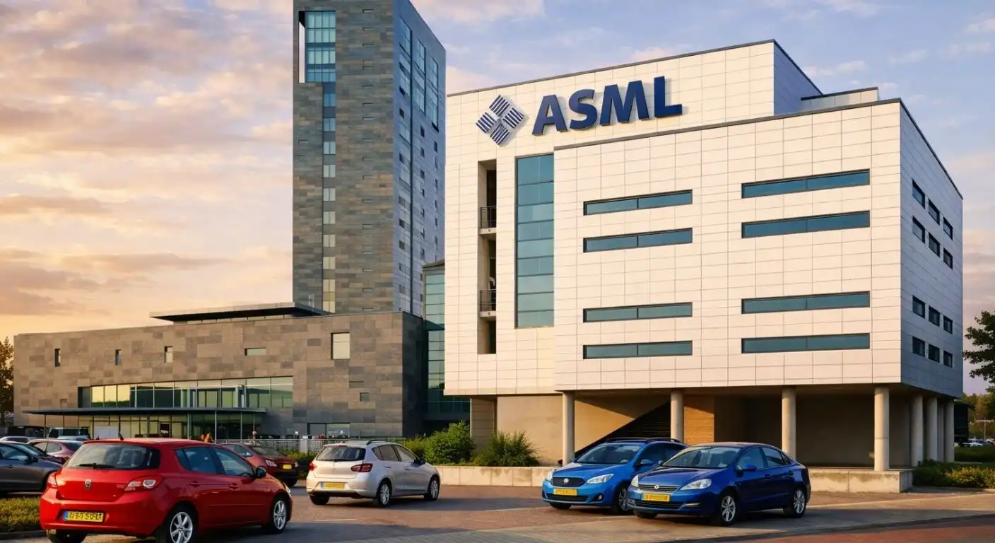
Deep inside ultra-clean, vibration-isolated manufacturing facilities in Veldhoven, Netherlands, Dutch technology titan ASML constructs the most complex, expensive, and irreplaceable industrial machine in human history. Costing over $250 million per unit, the ASML Twinscan NXE Extreme Ultraviolet (EUV) lithography system is the sole technology on Earth capable of printing the nanometer-scale transistors that power the global artificial intelligence revolution. Every cutting-edge artificial intelligence processor designed by Nvidia—including the 208-billion-transistor Blackwell B200, the GB200 NVL72 supercomputing rack, and upcoming Vera Rubin architectures—exists solely because this multi-million-dollar machine uses invisible beams of light to etch microscopic circuit lines onto silicon.
The physical and financial scale of ASML’s EUV technology defies standard industrial logic. A single $250 million machine weighs over 180 tonnes, incorporates more than 100,000 specialized components, utilizes 2 kilometers of high-purity fluid hoses, and requires 3 fully loaded Boeing 747 cargo planes, 13 transport containers, and 250 custom crates simply to ship to customer fabrication plants. Operating with a 100% global monopoly on extreme ultraviolet lithography, ASML functions as the ultimate physical gatekeeper of the modern digital economy, holding the master key to advanced microprocessors, high-bandwidth memory, and artificial general intelligence research.
As Big Tech hyperscalers commit over $200 billion annually in capital expenditures to build liquid-cooled data center clusters, global demand for ASML’s lithography systems has reached unprecedented heights. Leading semiconductor foundries—primarily Taiwan Semiconductor Manufacturing Company (TSMC), alongside Samsung Electronics and Intel—are competing aggressively to secure delivery slots for ASML’s tools. Without continuous shipments of these machines from the Netherlands to mega-fabs in Taiwan, Arizona, South Korea, and Texas, the global expansion of artificial intelligence hardware would come to an immediate, complete standstill.
TechGolly provides an in-depth technical and economic analysis of ASML’s $250 million lithography printer, evaluating extreme ultraviolet light physics, laser-produced plasma mechanics, Carl Zeiss sub-atomic optics, TSMC foundry integration, High-NA EUV advancements, and the geopolitical trade controls shaping global semiconductor supremacy.
Unpacking the Physics of 13.5-Nanometer Extreme Ultraviolet Light
To understand why a single manufacturing tool commands a $250 million price tag, semiconductor engineers and financial analysts must examine the extreme optical physics required to print modern microchips. For decades, chipmakers used deep ultraviolet (DUV) laser systems operating at a wavelength of 193 nanometers. However, as transistor features shrank below 7 nanometers, 193-nanometer light waves proved too wide, causing physical light diffraction that blurred microscopic circuit patterns.
To print features at 3-nanometer and 2-nanometer nodes, ASML engineered a system that operates at an extreme ultraviolet wavelength of just 13.5 nanometers—a light spectrum approaching the tiny dimensions of X-rays. Generating 13.5-nanometer EUV light at commercial power levels requires executing an extraordinary physics process known as Laser-Produced Plasma (LPP).
Inside the machine’s light source generator, a high-precision generator ejects 50,000 microscopic droplets of molten tin per second into a high-vacuum chamber, with each tin droplet measuring roughly 25 micrometers in diameter. A high-power industrial carbon dioxide laser—built by German laser specialist Trumpf—fires two precise, consecutive laser pulses at every single falling tin droplet.
The initial laser pulse flattens the microscopic tin droplet into a pancake shape. Microseconds later, the primary laser pulse strikes the flattened tin target with extreme intensity, heating the tin to over 400,000 degrees Celsius. The intense thermal energy vaporizes the tin instantly, converting it into a highly ionized plasma state that emits high-intensity 13.5-nanometer EUV photons. Executing this violent laser-plasma explosion 50,000 times per second generates a continuous, stable beam of extreme ultraviolet light.
Generating EUV light introduces a secondary physical constraint: extreme ultraviolet light is absorbed by almost all matter, including ambient atmospheric air and standard optical glass lenses. Consequently, the entire optical path inside ASML’s $250 million system—from the plasma generation chamber through the optical projection column down to the silicon wafer stage—must operate inside an ultra-high vacuum environment, completely devoid of air molecules.
Sub-Atomic Precision Optics: The Carl Zeiss Mirror Engineering
Because traditional glass lenses absorb 100% of extreme ultraviolet light, ASML had to completely abandon traditional refractive optics. Instead, the machine directs and focuses EUV light using a series of specialized reflective mirrors engineered by German optics pioneer Carl Zeiss.
Directing 13.5-nanometer light requires constructing multi-layer Bragg reflectors. Carl Zeiss crafts parabolic mirrors coated with 40 to 50 alternating atomic layers of molybdenum and silicon, with each individual layer measuring approximately 3.4 nanometers thick. These specialized atomic layers allow the mirror surface to reflect up to 70% of incoming EUV light through constructive interference, while absorbing the remainder as heat.
The physical smoothness required for these optical mirrors pushes the absolute boundaries of material science. Carl Zeiss polishes these parabolic mirrors using ion-beam milling, achieving surface smoothness tolerances measured at sub-atomic levels.
To visualize the extreme perfection of Carl Zeiss optics, optical engineers explain that if one of these projection mirrors were enlarged to the geographical size of the entire nation of Germany or the United States, the largest physical surface bump or defect on the mirror would measure less than 1 millimeter high.
This sub-atomic optical smoothness is necessary to prevent wavefront distortion as EUV light bounces across multiple mirrors in the projection column. The mirrors focus light onto the silicon wafer with nanometer-level precision, allowing chip foundries to print circuit lines that measure less than 20 silicon atoms in width.
Foundry Integration: How TSMC Converts ASML Light into Nvidia Chips
While ASML designs and builds the lithography tools in the Netherlands, the commercial realization of these machines occurs inside specialized mega-fabs operated by foundry giant TSMC in Taiwan and Arizona.
Inside TSMC’s flagship Fab 18 in Tainan, Taiwan, dozens of $250 million ASML EUV machines operate continuously inside Class-1 cleanroom halls where air filtration systems maintain near-zero dust particle counts. TSMC integrates ASML’s Twinscan NXE systems into its advanced 4-nanometer and 3-nanometer manufacturing lines, which produce 100% of Nvidia’s high-performance artificial intelligence processors.
The physical integration process between ASML’s machine and TSMC’s manufacturing process is extraordinarily precise. A 300-millimeter raw silicon wafer enters the ASML exposure chamber, where magnetic levitation dual-wafer stages accelerate the wafer with forces exceeding 10Gs. The dual-stage system positions the wafer beneath the optical exposure head with an overlay alignment accuracy better than 1.1 nanometers.
The machine exposes the silicon wafer, projecting the master circuit design from a quartz photomask onto a light-sensitive chemical photoresist applied to the wafer surface. Operating at peak operational speed, a single ASML EUV machine exposes over 160 silicon wafers per hour, completing hundreds of individual chip dies per wafer.
For Nvidia’s Blackwell B200 processor, the manufacturing requirements push physical limits. The Blackwell GPU consists of two reticle-limit silicon dies manufactured on TSMC’s 4-nanometer process node, connected by an ultra-high-speed 10-Terabyte-per-second interconnect fabric. Each individual B200 chip houses 208 billion transistors.
Once ASML tools print the complex circuit patterns on the silicon wafer, TSMC deploys its proprietary Chip-on-Wafer-on-Substrate (CoWoS) advanced packaging technology. CoWoS packaging places the two logic GPU dies side-by-side on a silicon interposer, surrounding them with 8 or 12 high-density stacks of High-Bandwidth Memory (HBM3e). The resulting unified processing unit delivers the massive floating-point mathematical performance required to train multi-trillion-parameter artificial intelligence models.
The Next Frontier: $380 Million High-NA EUV Systems
As semiconductor node scaling advances toward 2-nanometer and 1.4-nanometer process architectures, standard EUV lithography systems face physical resolution limits. To print even smaller transistor gates without relying on expensive, multi-exposure patterning loops, ASML developed its next-generation lithography platform: the Twinscan EXE High-NA EUV system.
The defining technical innovation of High-NA EUV is an increase in the optical numerical aperture (NA) from 0.33 to 0.55. Increasing the numerical aperture allows the optical system to capture higher-angle diffracted light, improving pattern resolution by 70% and enabling single-exposure printing of 8-nanometer transistor features.
To accommodate the larger 0.55 NA optics, Carl Zeiss designed massive anamorphic mirrors that are double the physical size of standard EUV mirrors. As a result, the High-NA EUV machine expands in physical size, weighing over 150 tonnes and requiring a dedicated two-story cleanroom hall to house its enlarged optical column and high-acceleration wafer stages.
The financial cost of High-NA EUV reflects its extreme engineering complexity. ASML prices each Twinscan EXE machine between $350 million and $380 million. Early adopters—including Intel, TSMC, and Samsung—have taken delivery of initial High-NA demonstration units, integrating the $380 million machines into research and development lines to prepare for mass production of 2-nanometer and 1.4-nanometer microchips in the late 2020s.
Supply Chain Bottlenecks, Logistics, and Geopolitical Chokepoints
The immense complexity of ASML’s $250 million lithography system makes the company dependent on a highly specialized, fragile global supply chain comprising over 5,000 niche industrial suppliers across Europe, North America, and Asia.
ASML operates primarily as a master architect and system integrator. Key specialized components are supplied by exclusive sole-source partners:
- Trumpf in Germany manufactures the ultra-high-power industrial CO2 lasers required to ignite the tin plasma.
- Carl Zeiss in Germany crafts the sub-atomic reflective mirror assemblies.
- Cymer in the United States engineers the high-frequency tin droplet generator modules.
- VDL Group in the Netherlands constructs the ultra-precision mechanical chassis and vacuum chambers.
Because these critical subsystems cannot be manufactured by any other company on Earth, a supply disruption at a single niche supplier can delay the final assembly and delivery of multi-hundred-million-dollar lithography tools.
This extreme supply chain concentration has made ASML the central battleground in the ongoing geopolitical technology war between the United States and China. Recognizing that access to advanced lithography dictates national artificial intelligence and military capabilities, the United States Department of Commerce partnered with the Dutch government to implement strict export controls on semiconductor equipment.
Under federal export regulations and Dutch licensing rules, ASML is legally prohibited from selling its extreme ultraviolet (NXE series) and advanced immersion deep ultraviolet (NXT series) lithography machines to Chinese foundries, including Semiconductor Manufacturing International Corporation (SMIC).
The trade restrictions were designed to freeze Chinese semiconductor capability at mature process nodes. However, losing access to foreign tools forced the Chinese government to launch a massive national self-reliance campaign. China registered the third phase of its National Integrated Circuit Industry Investment Fund (Big Fund III) with 344 billion yuan ($47.5 billion USD) in state capital, directing funds toward domestic toolmakers like Shanghai Micro Electronics Equipment (SMEE) to develop domestic 193-nanometer immersion DUV machines and alternative multi-patterning techniques.
Economic Unit Economics and the AI Infrastructure Supercycle
Evaluating the financial economics of advanced chip fabrication illustrates why chip foundries willingly pay $250 million to $380 million for a single ASML lithography tool.
Constructing a modern semiconductor mega-fab—such as TSMC’s Fab 18 in Taiwan or its expanding campus in Phoenix, Arizona—requires a total capital investment ranging between $15 billion and $20 billion. A single advanced fab facility houses 30 to 40 ASML EUV machines, representing a total lithography hardware investment exceeding $8 billion to $10 billion.
While initial capital expenditure is staggering, the long-term cash generation of an operational EUV mega-fab is unmatched in industrial manufacturing. Operating at 90%+ capacity utilization, a single TSMC 3-nanometer wafer fab processes over 100,000 300-millimeter silicon wafers per month. At average selling prices exceeding $20,000 per advanced wafer, a single mega-fab generates over $2 billion in monthly top-line revenue.
Furthermore, the commercial value of the finished artificial intelligence chips justifies the immense hardware investment. Nvidia sells its flagship Blackwell B200 and GB200 systems at premium gross margins exceeding 70% to 75%, with individual server boards commanding prices between $30,000 and $70,000.
Because technology hyperscalers are competing aggressively to build frontier reasoning models, the commercial demand for Nvidia’s AI chips remains virtually insatiable. Cloud providers willingly absorb high chip prices because deploying high-density AI compute generates high-margin recurring cloud subscription and API token revenues, creating a profitable financial feedback loop that validates ASML’s $250 million machine price tag.
Strategic Outlook for Global Semiconductor Manufacturing
As the global semiconductor industry moves toward 2-nanometer process architectures and 3D stacked gate-all-around (GAA) transistor designs, control over advanced lithography will remain the defining battleground of global industrial power.
Looking forward through the late 2020s, the semiconductor manufacturing ecosystem will operate under two distinct technological realities:
In Western nations and allied Asian manufacturing centers—specifically Taiwan, South Korea, Japan, the United States, and Western Europe—foundries will leverage ASML’s High-NA EUV systems to push monolithic silicon scaling down to sub-1-nanometer physical limits, building hyper-efficient microprocessors for artificial intelligence data centers, autonomous mobility, and mobile computing.
In mainland China, domestic foundries will operate localized, self-sustaining manufacturing loops, utilizing homegrown 193-nanometer immersion DUV machines, advanced multi-patterning algorithms, and 3D chiplet packaging to build capable artificial intelligence processors independently of Western equipment supply chains.
Despite ongoing research into alternative patterning techniques—such as nanoimprint lithography or directed self-assembly—no alternative technology can match the processing throughput, pattern density, and yield reliability delivered by ASML’s extreme ultraviolet systems.
ASML’s $250 million lithography machine will remain the fundamental physical foundation holding up the entire global artificial intelligence economy, proving that in the 21st century, control over extreme optical physics is equivalent to control over the future of human computing.
Key Takeaways for Tech Executives, Chip Designers, and Investors
The central role played by ASML’s $250 million lithography systems delivers vital strategic lessons for executive decision-makers, technology architects, supply chain directors, and global institutional investors.
First, physical hardware infrastructure dictates the boundaries of digital software innovation. Technology leaders must recognize that artificial intelligence software scaling relies fundamentally on a fragile physical supply chain anchored by a single equipment manufacturer in the Netherlands.
Second, semiconductor equipment supply chain tracking is an essential investment metric. Global capital allocators and technology analysts must track ASML tool shipment volumes, lead times, and TSMC capital expenditure plans as the primary leading indicator for future AI hardware availability and tech sector earnings growth.
Third, geopolitical trade policy has permanently altered global manufacturing strategy. Technology companies must build resilient, multi-region hardware supply chains, preparing for a bifurcated global semiconductor market where Western high-NA EUV foundries co-exist alongside domestic Chinese mature-node ecosystems.
Finally, the semiconductor supercycle is an irreplaceable long-term growth engine. As artificial intelligence, autonomous vehicles, industrial robotics, and clean energy grids demand trillions of additional microprocessors, companies that own, operate, or supply the physical equipment required to print silicon will capture sustained corporate value for decades to come.