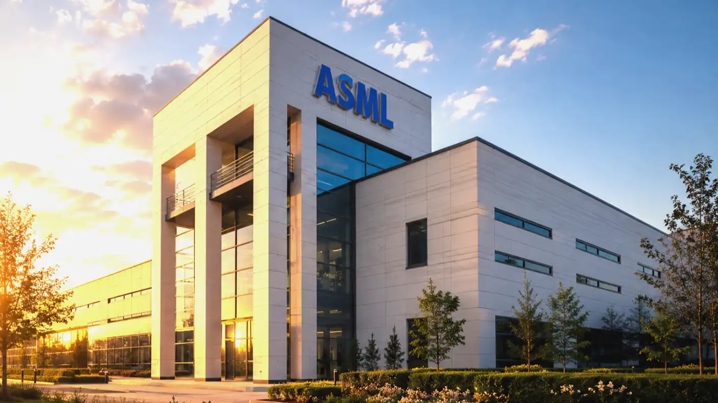
The global semiconductor market has entered its most aggressive, highly competitive phase. While financial markets have spent much of the year focused on the high-profile earnings beats of chip designers and the massive data center buildouts of cloud providers, the physical execution of this entire technological revolution is built on a highly specialized foundation of advanced manufacturing equipment. In a bold, unprecedented corporate maneuver designed to secure its highly coveted workforce, Dutch lithography giant ASML Holding NV has launched a massive employee retention initiative.
According to an internal corporate memo distributed recently on a Monday in mid-July, the company’s newly appointed Chief Executive Officer, Christophe Fouquet, announced that ASML will offer a €20,000—approximately $21,800—cash bonus to the vast majority of its global workforce. The primary objective of the program is to retain the company’s highly trained, specialized technicians, optical scientists, and software engineers through December 31, 2030. This long-term commitment represents a massive, €800 million capital outlay that demonstrates how valuable and scarce semiconductor engineering talent has become in the modern digital era.
By establishing the ASML Employee Retention Bonus Program, the company is directly addressing the realities of a global technology arms race. As the world’s only manufacturer of extreme ultraviolet lithography systems, ASML has become the indispensable gatekeeper to the modern digital world. However, this absolute monopoly has turned the company into a primary target for competitors looking to build their own advanced chip-making programs. By locking in its workforce with a guaranteed, long-term financial incentive, the company is building a highly effective, human-capital shield to protect its proprietary engineering secrets and ensure it can deliver on its ambitious growth targets.
The Global Semiconductor Talent War: Why ASML Must Protect Its Brain Trust
To understand why the company is willing to spend nearly a billion dollars on employee bonuses, investors must look at the extreme scarcity of labor within the semiconductor industry. Operating an advanced wafer fab equipment business is not a traditional manufacturing process that can be easily automated or staffed with low-skilled workers. It is an incredibly complex, deep-tech discipline that requires an extraordinary level of specialized scientific knowledge.
An ASML extreme ultraviolet lithography machine is widely considered the most complex commercial device ever engineered. A single system consists of more than 100,000 individual parts, 3,000 cabling systems, and requires three chartered Boeing 747 cargo planes to ship to a customer’s factory.
Because the machinery operates at the absolute limit of physical possibility—using high-power lasers to vaporize molten tin droplets 50,000 times a second to generate the extreme ultraviolet light needed to print sub-2-nanometer silicon features—the engineers who build, align, and service these tools are some of the most sought-after professionals on Earth.
A newly hired engineer typically requires up to three years of intensive, on-the-job training before they can comfortably operate or service a single subsystem of an EUV machine.
This long training period means that losing an experienced, mid-level engineer to a competitor is an incredibly expensive setback for the company.
Industry analysts estimate that the total cost of losing a senior hardware engineer—including lost productivity, recruiting overhead, and training expenses—can easily exceed $1 million per individual.
With global rivals like TSMC, Samsung, Intel, and emerging, state-subsidized Chinese players aggressively hunting for talent, ASML’s human capital has become its most critical, highly vulnerable asset.
The Competitor Threat: The Bait of Silicon Valley and East Asia
The competitive pressure on ASML’s talent pool is particularly acute from major international foundries and chip designers. As companies like TSMC and Samsung construct massive new advanced manufacturing facilities in the United States, Europe, and Japan, they are locked in their own high-stakes battle to recruit the specialized technicians needed to run their new cleanrooms.
These global giants are willing to pay massive premiums to attract experienced workers.
They frequently target ASML’s field service engineers, who spent years working inside their facilities and possess direct, hands-on experience in optimizing lithography tools for high-volume manufacturing.
By offering large signing bonuses, housing subsidies, and highly competitive stock-option packages, these rivals are attempting to drain ASML’s brain trust.
The €20,000 retention program acts as a direct counter-measure, giving employees a powerful, long-term financial incentive to ignore recruiters’ calls and stay committed to the company’s long-term roadmap.
The Geopolitical Threat of Technology Leakage
The talent war also carries profound national security implications. As the United States and the European Union implement strict export controls to prevent advanced semiconductor technologies from entering China, the Chinese government has launched an aggressive, state-supported campaign to build its own domestic lithography alternatives.
Because building these systems from scratch is an incredibly difficult scientific hurdle, Chinese state-backed startups are highly incentivized to recruit experienced Western engineers.
If a competitor can recruit even a handful of senior optical or laser specialists from ASML’s laboratories, they can potentially leapfrog years of expensive research and development.
This has made ASML’s workforce a primary target for sophisticated industrial espionage and aggressive foreign recruiting.
By securing its engineers through 2030, the company is protecting both its own competitive advantages and the national security interests of Western nations, ensuring that the critical, high-precision engineering skills required to build advanced silicon remain safely within its regulated network.
Underwriting the Thirty-Percent Capacity Expansion Plan
The decision to launch the retention program is directly connected to the company’s ambitious long-term operational plans. In its recent, record-breaking second-quarter earnings report, the company announced that it plans to expand its tool manufacturing capacity for both its flagship EUV and Deep Ultraviolet machines by 30% in each of the next two years, covering 2027 and 2028.
This massive physical expansion represents an extraordinary capital commitment, designed to satisfy the insatiable global demand for advanced artificial intelligence chips.
However, achieving this 30% expansion target is physically impossible if the company suffers from high employee turnover or struggles to find enough experienced workers to staff its new assembly lines.
The company needs every single experienced hand on deck to manage the complex logistics of the capacity ramp, making the retention of its existing workforce a matter of absolute, near-term operational survival.
The Non-Executive Bonus Distribution and Financial Scale
The structure of the €20,000 retention program is designed to maximize its impact on the factory floor. The company has explicitly excluded senior executives from participating in the program, choosing instead to distribute the cash exclusively to its non-executive workforce, which includes more than 40,000 eligible employees across its global operations.
Under the terms of the internal memo, eligible employees who remain on the active payroll through December 31, 2030, will receive the lump-sum payment of €20,000.
This targeted distribution is a highly efficient way to build loyalty among the mid-level engineers, cleanroom technicians, and software developers who actually build, test, and ship the massive lithography machines.
While spending up to €800 million ($870 million) over the next four years represents a significant capital outlay, it is a highly predictable, manageable expense that is far cheaper than the potentially catastrophic costs of delayed machine shipments, engineering errors, or lost market share to more agile competitors.
Improving Employee Morale and Operational Consistency
The rollout of the retention bonus also serves to improve employee morale and operational consistency during a period of high organizational stress. Ramping up machine production by 30% annually places immense physical pressure on the factory workforce.
Employees must work longer shifts, manage more complex supply chain schedules, and adapt to constant, rapid engineering updates on the assembly line.
In this high-pressure environment, burnout and employee fatigue are major risks.
By offering a guaranteed, non-diluted €20,000 bonus, the company’s leadership team is providing a powerful, highly visible form of recognition for the hard work of its employees.
This financial incentive improves morale, fosters a strong sense of collective purpose, and ensures that the company maintains the high operational consistency required to print microscopic features on silicon wafers with absolute, zero-error precision.
Operation Beethoven: The Dutch Government’s Two-Billion-Euro Rescue
The corporate decisions made by the company’s executive board do not exist in a vacuum; they are deeply supported by the national policies of the Dutch government. For several years, the company’s leadership team expressed growing concern that the political and social environment in the Netherlands was becoming increasingly hostile to technological growth.
The rise of populist, anti-immigration political movements in the country threatened the company’s ability to hire the skilled foreign workers who account for a significant percentage of its highly specialized engineering workforce.
Furthermore, a severe housing shortage and a lack of investment in public infrastructure in the Eindhoven region made it difficult for the company to attract and retain international talent.
Faced with these structural bottlenecks, the company’s previous leadership team issued a stark warning to the government, threatening to expand its operations overseas if the domestic business environment did not improve.
Upgrading the Eindhoven Technological Cluster
The Dutch government took the company’s warning with absolute seriousness, recognizing that losing its most valuable technology champion would represent a catastrophic blow to the country’s economic future.
In response, the Hague launched “Operation Beethoven,” a massive, €2.5 billion ($2.7 billion) federal funding package designed specifically to keep the company’s headquarters and primary research hubs anchored in the Netherlands.
The multi-billion-euro funding package is being used to upgrade the entire technological and social infrastructure of the Eindhoven region:
- Expanding Technical Education: Funding massive expansions of the technical programs, laboratories, and research departments at the Eindhoven University of Technology to double the local graduate pipeline.
- Constructing Affordable Housing: Building thousands of new, modern residential apartments to house the incoming wave of local and international technology workers.
- Upgrading Regional Infrastructure: Expanding high-capacity public transit networks, electrical grids, and road systems to support the rapid growth of the local technology cluster.
- Securing Favorable Labor Policies: Adjusting national tax codes and visa regulations to ensure that high-tech companies can continue to hire qualified foreign workers with minimal administrative friction.
By pairing the government’s €2.5 billion infrastructure support with its own €800 million employee retention program, the company is building an impenetrable competitive fortress.
It is ensuring that Eindhoven remains the premier, undisputed capital of the global semiconductor research world, providing its engineering teams with a world-class environment to live, work, and invent the technologies of the future.
The Future of American and European Deep Tech
As the global technology sector continues to navigate a highly volatile, politically walled geopolitical landscape, the successful execution of the company’s retention program represents a major milestone for Western technological sovereignty.
The battle for advanced semiconductor dominance is no longer just about who has the largest capital budget; it is a battle for human capital and raw engineering talent.
By securing its core workforce through 2030, the company is ensuring that its next-generation “High-NA” and “Feynman” development programs remain fully staffed and completely on schedule.
These advanced projects are essential for supporting the ongoing artificial intelligence revolution, as they will allow chipmakers to print the sub-1-nanometer transistor features required to build the supercomputers of the future.
As other global technology companies adapt to this new era of tech-talent scarcity, the company’s proactive, highly disciplined approach to employee retention will serve as a valuable blueprint, proving that the real power of a tech giant resides not in the physical steel and concrete of its factories, but in the collective, irreplaceable minds of the human beings who write the code and design the machines that power our world.