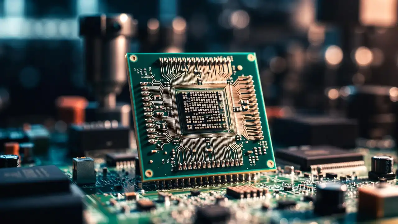
The global semiconductor manufacturing landscape is approaching a critical, material-science bottleneck. For decades, chipmakers followed the traditional parameters of Moore’s Law, doubling computing power every two years by systematically shrinking the size of silicon transistors. Today, however, these microscopic circuits are hitting their absolute physical and thermal limits, fanning a severe “power wall” that threatens to derail the artificial intelligence revolution. In response, the industry’s focus is rapidly turning from transistor design to advanced materials science, with Japan chip startup Gaianixx emerging as a prominent pioneer.
Founded in 2021 as a high-tech spinout from the University of Tokyo, Gaianixx is developing revolutionary single-crystal thin-film technology designed to resolve one of the most fundamental material challenges in the semiconductor industry. By utilizing a proprietary, multifunctional interlayer film, the startup has made it possible to stack and grow completely dissimilar, difficult-to-layer materials directly onto standard silicon wafers without creating structural defects or cracking, establishing a highly resilient, physical defense against the thermal limitations of modern computing.
As global technology giants scramble to build out their artificial intelligence data centers, the demand for Gaianixx’s advanced material solutions is growing at a rapid pace. The startup’s innovative technology has already secured substantial financial backing from leading Japanese venture capital firms and industrial materials giants, positioning the Tokyo-based company to play a critical role in the global semiconductor supply chain and proving that the next major breakthrough in AI will be won in the materials laboratory.
The Mechanics of Gaianixx’s Breakthrough Materials Technology
The core technological breakthrough developed by Gaianixx is its proprietary epitaxy technology, which allows manufacturers to grow high-quality single crystals in a multi-layered structure on standard silicon substrates.
Overcoming the Physical Barrier of Lattice Mismatch
In the semiconductor manufacturing process, growing a thin film of one material on top of another substrate is a standard procedure. However, if the two materials possess different crystalline structures or atomic spacings—known as different lattice constants—the atoms will not align properly at the interface. This structural discrepancy, known as a lattice mismatch, creates severe mechanical stress within the chip, leading to atomic dislocations, structural defects, and eventually, physical cracking that renders the chip completely non-functional.
This physical barrier has prevented chipmakers from integrating advanced, high-performance materials directly onto standard silicon wafers.
For instance, materials like piezoelectric crystals, which convert mechanical stress into electrical energy, and ferroelectric oxides, which are essential for advanced computer memory, possess atomic lattices that are highly incompatible with silicon.
As a result, manufacturers had to build these components on separate, expensive specialized substrates, which increased production costs and restricted their computational performance.
The Science of Dynamic Lattice Matching Interlayers
Gaianixx has successfully resolved this long-standing materials bottleneck by developing an innovative, multifunctional interlayer film. This specialized film, applied directly to the silicon wafer before the growth process begins, utilizes a dynamic lattice matching mechanism to act as an atomic cushion.
The dynamic interlayer automatically adjusts its atomic spacing to accommodate the different lattice constants of the two dissimilar materials, absorbing the mechanical stress and preventing the formation of dislocations or cracks.
This breakthrough enables the flawless growth of ultra-high-quality, single-crystalline thin films on standard silicon substrates.
By allowing manufacturers to stack previously incompatible materials directly onto cheap, high-volume silicon wafers, the technology significantly lowers production costs while unlocking unprecedented levels of device performance and design flexibility.
Solving the AI Power Wall: Turning Silicon into a Neuromorphic Playground
The commercial significance of Gaianixx’s technology is closely linked to the massive, energy-intensive requirements of the global artificial intelligence boom, where traditional silicon architectures are struggling to cope with the rising power demands.
Shifting from Electric Packets to Magnetic Electron Spin
Modern computer chips rely on the physical movement of electrical packets, or electrons, through copper wires to represent and process binary information. While this electronic model has been highly successful, the constant movement of electrons generates significant friction, resulting in immense heat generation and thermal energy loss that limits the performance of advanced processors.
To bypass this thermal “power wall,” researchers are developing next-generation spintronic and neuromorphic (brain-mimicking) computing devices. Spintronics explores the possibility of storing and processing information using the magnetic spin of electrons rather than their electrical charge, which produces virtually zero heat and operates at near light speed.
However, manufacturing these advanced spintronic devices requires growing ultra-high-quality single-crystalline magnetic and ferroelectric thin films directly on silicon wafers—a process that was physically impossible before the development of Gaianixx’s dynamic buffer layers.
Reaching for Hundred-Fold Gains in Computational Efficiency
By utilizing Gaianixx’s advanced interlayers, research teams at the University of Tokyo have successfully demonstrated the fabrication of large-area, single-crystalline ferroelectric oxide thin films on standard silicon substrates.
By intentionally introducing oxygen vacancies into these advanced thin films, researchers discovered the emergence of giant resistive switching and memristive properties, which are essential for building neuromorphic devices.
The computational and energy benefits of this technology are historic.
Because these advanced spintronic and memristive devices do not rely on traditional, heat-heavy electrical currents, they can store and process information while consuming only a fraction of the power required by conventional silicon chips.
Research models project that scaling up this technology could deliver up to a 100-fold improvement in power and computational efficiency, providing a highly effective solution to the massive energy crisis currently facing global AI data centers, and proving that even a 1.5% improvement in processing latency or a 1.5% reduction in administrative delays can save manufacturers billions of dollars annually.
The Corporate Footprint: Securing Two Billion Yen in Series C Funding
The high-tech potential of Gaianixx’s materials technology has allowed the startup to secure substantial financial backing from some of the most influential venture capital firms and industrial materials groups in Japan.
From University of Tokyo Laboratories to the Global Market
Gaianixx was originally founded in November 2021 by CEO Kento Nakao, who wanted to commercialize the advanced single-crystal thin-film research developed within the laboratory of Professor Satoru Nakatsuji at the University of Tokyo’s Institute for Solid State Physics.
By establishing a close, collaborative relationship with the university’s technology transfer office, the startup successfully transitioned the technology from academic research into a highly valuable commercial asset.
The company’s rapid corporate growth is a primary example of Japan’s emerging, university-backed startup ecosystem.
By combining academic engineering excellence with private venture capital, the firm has built a highly scalable business model, establishing corporate headquarters in Tokyo and actively marketing its advanced single-crystal wafers to global semiconductor companies.
Backed by Japan’s Prominent Materials and Venture Capital Giants
The financial strength of the company was on full display recently when Gaianixx officially announced the successful completion of a 2 billion yen (approximately $12.7 million) Series C funding round.
This massive capital injection brought the startup’s total funding raised to date to a substantial level, providing it with the resources needed to scale its operations.
The Series C round drew investments from a powerhouse coalition of strategic and financial backers, including:
- University of Tokyo Edge Capital Partners (UTEC): The university’s flagship deep-tech fund, which has supported the company since its seed rounds.
- JX Advanced Metals Corporation: A global leader in semiconductor materials, sputtering targets, and high-purity copper foil, which entered the round as a key strategic partner.
- JIC Venture Growth Investments: A government-backed venture fund designed to support high-growth technology innovators.
- SMBC Venture Capital and i-nest Capital: Prominent private financial venture funds.
- JSR Active Innovation Fund: The venture arm of semiconductor materials giant JSR Corporation, which was acquired and taken private by the Japanese government in 2024 for $6.4 billion.
Gaianixx plans to utilize the net proceeds from this massive funding round to accelerate its manufacturing and product qualification schedules.
The company is constructing advanced, commercial-scale pilot lines to produce its customized single-crystal wafers, ensuring it can deliver high-volume orders to global semiconductor clients and help them navigate the physical and thermal limits of the AI age.
The Broad-Based Materials Pivot: Reclaiming Japan’s Tech Sovereignty
The success of Gaianixx is part of a broader, highly coordinated national campaign in Japan to reclaim its historic position as a global semiconductor superpower.
Japan’s Silent Monopoly Over the Semiconductor Chemical Stack
While the global media often focuses on the high-profile chip fabrication battles between TSMC, Samsung, and Intel, industry insiders recognize that the entire global semiconductor industry remains completely dependent on Japanese materials and equipment.
During the “lost decades” of the 1990s and 2000s, when Japanese companies lost their dominant share of the high-volume computer chip market to rivals in Taiwan and South Korea, Japanese firms quietly pivoted, establishing a silent monopoly over the underlying chemical stack.
Today, Japan controls more than half of the global market for semiconductor manufacturing materials, including photoresists, silicon wafers, high-purity gases, and advanced packaging substrates.
Without these Japanese materials, no advanced chip factory in Taiwan, South Korea, or the United States can operate, giving Japan immense geopolitical leverage in the global technology race.
By supporting high-tech startups like Gaianixx, the government is ensuring that this critical materials-science lead remains secure, building a highly resilient, self-reliant technological base.
The Rapidus Consortium and the Two-Nanometer 2027 Target
To complement its materials dominance, Japan is also investing heavily to rebuild its domestic manufacturing capabilities through Rapidus, a government-backed semiconductor consortium funded by the state and 32 private-sector giants, including Sony, Toyota, and SoftBank.
Rapidus has announced an audacious plan to leapfrog from legacy 40-nanometer production to cutting-edge 2-nanometer logic chips by 2027, constructing a state-of-the-art fully automated fabrication plant in Chitose, Hokkaido.
The consortium’s strategy is not to outproduce TSMC on sheer volume, but to focus on speed, delivering custom, high-performance AI chips under much shorter turnaround times.
By combining Rapidus’s advanced manufacturing lines with Gaianixx’s breakthrough single-crystal materials technology, Japan is building a highly integrated, sovereign technology ecosystem, preparing itself to lead the next century of global computing and securing large-scale industrial projects requiring over $1 billion in capital investments.
Engineering the Visual and Physical Future of Technology
The successful completion of the Series C funding round and the commercial expansion of Japan chip startup Gaianixx represent a historic milestone in the modern history of the semiconductor industry. By utilizing its revolutionary CMOS directly bonded to Array and dynamic lattice matching technologies, the University of Tokyo spinout has proven that the materials laboratory is the ultimate frontier of the artificial intelligence revolution.
While the competitive pressures from global foundry giants remain intense, Gaianixx’s unique ability to stack previously incompatible, high-performance materials directly onto cheap silicon wafers provides it with a powerful, unassailable economic moat.
As the company continues to construct its advanced manufacturing lines and qualify its customized wafers for global clients, its technology will ensure that the physical systems of the modern age can successfully bypass the thermal limits of silicon.
This strategic materials breakthrough will ensure that Japan remains the undisputed leader of the global technology supply chain, providing the world with the advanced, energy-efficient building blocks required to power the automated, connected, and highly sovereign future of global commerce.