Key Points:
- Japanese chipmaker Kioxia is holding a ceremony at its Kitakami K2 facility to prepare for the mass production of its 10th-generation 332-layer BiCS FLASH memory.
- The rapid shift of AI workloads toward local inference has triggered an explosion in demand for high-capacity flash storage, completely selling out Kioxia’s 2026 capacity.
- Driven by this historic turnaround, Kioxia’s stock has surged over 670 percent in 2026, overtaking Toyota as Japan’s most valuable company.
- The Kioxia-SanDisk alliance is boosting capital expenditure by 41 percent to $4.5 billion to support rapid scaling of advanced 3D NAND technology.
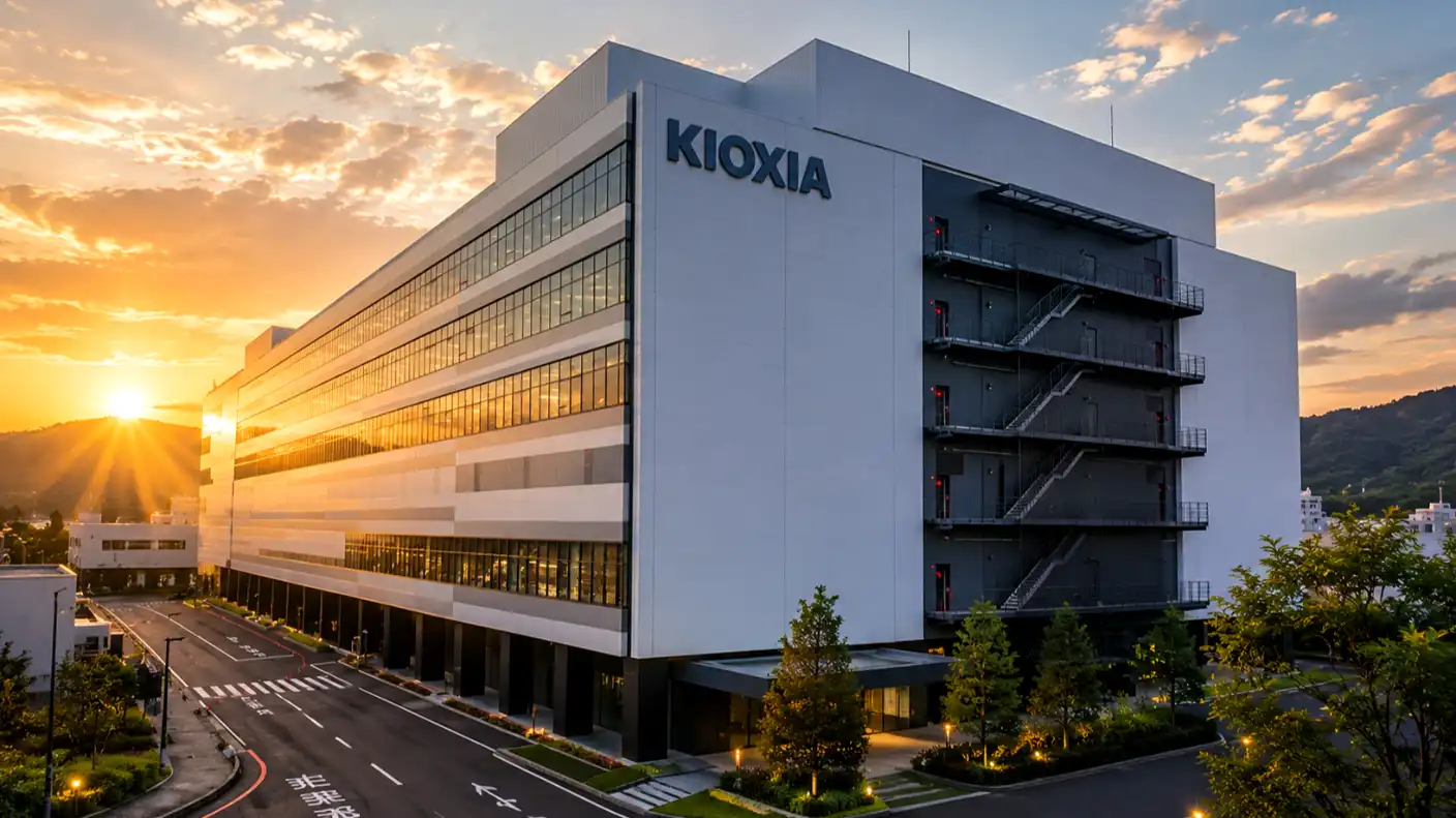
A historic, highly dramatic industrial resurrection is taking shape in the global semiconductor sector. Japanese chipmaker Kioxia is hosting a milestone ceremony on Friday at its state-of-the-art K2 fabrication facility in Kitakami, northern Japan, to prepare for the high-volume manufacturing of its next-generation flash memory. Driven by the explosive global artificial intelligence boom, the company has executed a spectacular corporate turnaround, transitioning from a heavily indebted, struggling legacy business into the hottest commodity play in the tech sector. By fast-tracking its manufacturing timelines to capture a massive regional supply deficit, the firm has established itself as the ultimate partner powering the next phase of the computing revolution.
The primary catalyst behind this dramatic corporate comeback is a structural shift in how global technology companies deploy artificial intelligence. While the initial phase of the AI boom focused almost exclusively on the training of massive language models, which heavily prioritized Nvidia’s graphics chips and high-bandwidth memory (HBM), the market is now moving rapidly into the “inference” and localized execution phase. Running these trained models to serve millions of daily user requests requires immense, high-performance, and ultra-high-capacity storage. This technical necessity has triggered a massive, global demand wave for advanced 3D NAND flash storage to prevent system bottlenecks and process massive vector databases in real time.
This massive demand wave has completely outstripped the company’s available manufacturing output. In official corporate updates, Kioxia confirmed that its entire NAND flash production capacity for 2026 is already completely sold out, with the severe supply-demand imbalance expected to persist well into 2027. Rather than selling its highly sought-after storage wafers to the highest bidder on the spot market, the chipmaker has implemented a disciplined allocation policy. The company is prioritizing its long-term, strategic hardware partners to ensure stable, reliable deliveries, completely shielding them from sudden market gluts while establishing a highly predictable, long-term revenue stream.
The financial market’s reaction to this technical turnaround has been nothing short of spectacular. Kioxia’s stock, which recently went public on the Tokyo Stock Exchange after several delays, has surged by a staggering 670% in 2026 alone. This astronomical rally has pushed the company’s total market capitalization past major domestic milestones, allowing the memory maker to officially claim the title of Japan’s most valuable public company from automotive giant Toyota. This historic “changing of the guard” in Tokyo proves that investors are fully prepared to assign premium, trillion-yen valuations to companies that control the physical infrastructure of the AI age.
The technological cornerstone of this market dominance is the company’s revolutionary 10th-generation BiCS FLASH 3D NAND architecture, also known as BiCS10. Built using advanced CMOS directly Bonded to Array (CBA) technology, the new chips feature an extraordinary 332-layer stacking structure, representing a massive 38% increase over its previous 218-layer design. This advanced structural engineering delivers a massive 59% increase in overall storage density, allowing developers to pack tens of terabytes of secure storage onto a single, standard enterprise solid-state drive. Furthermore, the chips deliver a blazing-fast data transfer speed of 4.8 gigabytes per second, representing a 33% performance improvement.
To bring this cutting-edge technology to market far ahead of its competitors, the company has bypassed the long, expensive process of constructing a brand-new factory. Instead of waiting years for fresh cleanrooms, the manufacturer has chosen to completely repurpose its newly operational K2 facility in Kitakami, which originally began manufacturing in September. This clever operational pivot has allowed the chipmaker to advance the mass production timeline of its 332-layer BiCS10 memory by more than a year, moving the commercial launch from late 2027 to the current fiscal year to satisfy the immediate demand from cloud hyperscalers and data centers.
This aggressive technological acceleration is backed by a massive capital investment campaign executed in tandem with its long-term joint-venture partner, Western Digital’s SanDisk. The U.S.-Japan NAND alliance is boosting its total capital expenditure by a massive 41% year-on-year to reach $4.5 billion in 2026. This significant financial war chest is dedicated entirely to expanding the production of its 8th-generation BiCS8 chips while accelerating research and development on its next-generation BiCS9 and BiCS10 lines. By investing aggressively while other major memory makers remain cautious about expanding NAND capacity, the alliance is successfully reasserting its dominance in the global storage market.
The company’s dramatic rise is also a massive victory for its primary private equity backer, Bain Capital, which led a historic $18 billion buyout to acquire the memory business from a struggling Toshiba Corporation back in 2018. Following the acquisition, the private equity firm faced years of severe market downturns, corporate restructuring, and delayed initial public offering plans that led many commentators to write off the investment as a failure. By maintaining strict financial discipline and supporting the company’s long-term R&D, Bain has successfully turned the business into a multi-billion-dollar powerhouse. The firm is now preparing for a secondary U.S. listing in spring 2027 to tap into deeper global capital pools.
Ultimately, the successful launch of Kioxia’s next-generation mass production lines demonstrates that the AI revolution has officially graduated from a software experiment into a highly physical, hardware-constrained battle. While software developers continue to design increasingly complex algorithms, running these models in real-world applications requires an astronomical volume of physical, high-speed storage. By fast-tracking its 332-layer technology and securing multi-year contracts with global hyperscalers, the Japanese pioneer has proved that it holds the keys to the future of smart computing. The semiconductor landscape is shifting, and the companies that control the physical storage layers will continue to lead the way.