

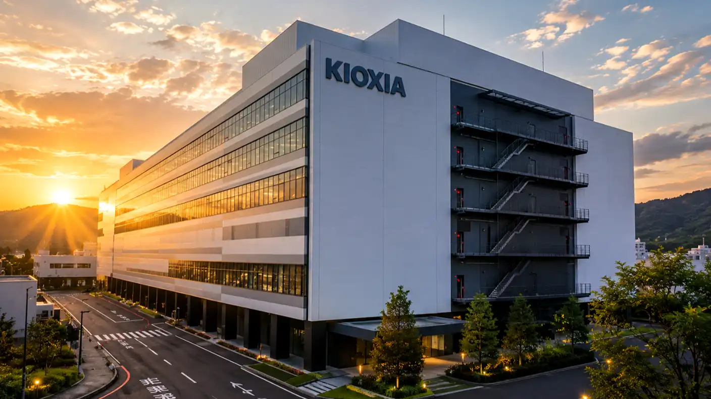
Key Points:
- Japanese memory chipmaker Kioxia Holdings plans to invest over 1 trillion yen ($6.27 billion) to construct a new manufacturing facility in northern Japan.
- The new fabrication building at the Kitakami Plant in Iwate Prefecture will mass-produce next-generation 332-layer 3D NAND flash memory.
- The expansion addresses a global flash storage shortage driven by explosive growth in artificial intelligence data centers and cloud computing.
- Kioxia aims to increase its annual capital expenditure by 66% through fiscal 2028 to secure long-term enterprise supply agreements.
Japanese semiconductor manufacturer Kioxia Holdings is launching a massive capital expansion to reinforce its position in the global memory market. The company plans to invest more than 1 trillion yen, equivalent to approximately $6.27 billion, to construct an advanced manufacturing facility at its flagship production plant in northern Japan. The multi-billion-dollar investment aims to scale up the production of next-generation 3D NAND flash memory chips to feed insatiable global demand from artificial intelligence data centers and hyperscale cloud providers.
The new production facility will be built within the company’s expanding Kitakami Plant located in Iwate Prefecture. The Kitakami manufacturing complex currently operates two large-scale fabrication facilities. The original Fab 1 commenced commercial manufacturing in 2020, while the newer Fab 2 entered service late last year to produce advanced 10th-generation 332-layer BiCS FLASH memory. The planned third building will extend the campus footprint significantly, creating expansive cleanroom space to house advanced lithography and etching equipment.
The technological focus of the upcoming facility centers on extremely high-density flash storage. Next-generation 332-layer 3D NAND flash architecture stacks hundreds of microscopic memory cells vertically, delivering massive storage capacity within an ultra-compact silicon die. These advanced chips form the core building blocks for high-capacity enterprise solid-state drives, which data center operators deploy in high-density server racks to feed massive datasets into artificial intelligence training clusters and real-time inference engines.
The massive capital outlay arrives amid a severe worldwide shortage of memory and storage silicon. As technology conglomerates and cloud providers accelerate investments in artificial intelligence infrastructure, global demand for high-speed enterprise storage has far outpaced available manufacturing capacity. Industry supply chain data indicates that global NAND flash supply growth is running at roughly 17% this year, falling well short of projected demand growth exceeding 20%, creating a persistent structural deficit across international hardware markets.
The decision to expand cleanroom capacity follows a dramatic financial turnaround for the Japanese chipmaker. After weathering cyclical downturns in previous years, the company has benefited from skyrocketing flash memory prices, with corporate operating margins recently surging past 70%. Having effectively sold out its manufacturing capacity through the end of the year, the enterprise is leveraging its strong pricing power and soaring cash flows to fund long-term factory expansions.
The new Kitakami facility represents a core component of the company’s medium-term investment roadmap. Corporate planners intend to increase average annual capital expenditures by 66% through fiscal 2028, allocating hundreds of billions of yen annually to upgrade production lines and secure advanced wafer fabrication machinery. To insulate the business from historical commodity boom-and-bust cycles, the enterprise plans to transition at least 50% of its total flash shipments into multi-year long-term supply agreements with major global cloud clients.
The project also builds upon the company’s long-standing industrial partnership with American flash storage maker SanDisk. For more than 25 years, the two companies have jointly operated and funded fabrication facilities across Japan, including the massive Yokkaichi manufacturing complex in Mie Prefecture and the Kitakami site. Under their shared manufacturing framework, the partners split equipment capital costs and divide finished silicon wafer output, allowing both firms to achieve high economies of scale while reducing individual balance sheet risk.
The multi-billion-dollar expansion aligns directly with Japan’s broader industrial strategy to rebuild its domestic semiconductor ecosystem. The Japanese government has implemented substantial financial subsidies and tax credits to revitalize domestic chipmaking, aiming to triple domestic semiconductor sales to past 15 trillion yen by 2030. Expanding advanced NAND flash fabrication in Iwate Prefecture strengthens sovereign technology supply chains and reduces reliance on foreign semiconductor foundries during periods of international trade friction.
As the global digital economy transitions from traditional cloud storage toward data-intensive artificial intelligence workflows, reliable access to high-density flash memory has become an essential pillar of technological power. By committing over 1 trillion yen to build its newest fabrication facility in Kitakami, Kioxia is establishing a robust manufacturing foundation to challenge international competitors like Samsung Electronics and SK Hynix. The massive investment ensures that Japan remains at the forefront of the global semiconductor supercycle for the decade ahead.