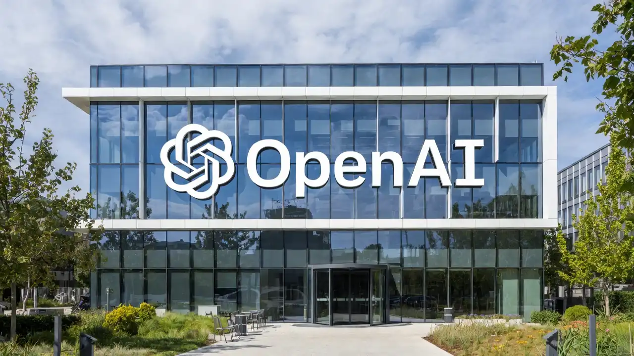
OpenAI has announced a major technological breakthrough, revealing that its first generation of custom-designed artificial intelligence processors outperforms flagship Nvidia hardware in internal benchmark evaluations. The disclosure marks a pivotal moment in the global semiconductor landscape, proving that the world’s leading generative artificial intelligence laboratory can design high-performance silicon capable of challenging Nvidia’s dominant market monopoly.
Internal testing data reveals that OpenAI’s custom application-specific integrated circuits achieve up to 2.8 times higher token throughput per watt and reduce inference latency by more than 40% compared to current-generation commercial graphics processing units. Developed in close technical collaboration with semiconductor designer Broadcom and fabricated on Taiwan Semiconductor Manufacturing Company’s advanced 3-nanometer node, the proprietary chips are engineered specifically to run massive frontier reasoning models and complex agentic workflows.
The engineering milestone arrives as frontier laboratories face soaring operational expenses. OpenAI spends billions of dollars every year renting server capacity from cloud providers to power conversational queries, video generation, and autonomous software agents. By deploying custom silicon across partner data centers, OpenAI aims to slash its cost-per-token expenses, protect its balance sheet, and take direct control over the physical compute infrastructure that powers the future of artificial intelligence.
A Historic Breakthrough in Custom Artificial Intelligence Silicon
For years, the artificial intelligence industry operated under the assumption that designing custom silicon to compete with Nvidia was nearly impossible for software-focused research labs. Nvidia’s multi-decade head start in hardware design, combined with its entrenched CUDA software programming ecosystem, created a formidable barrier to entry.
OpenAI broke through this barrier by assembling an elite hardware engineering division comprising veteran chip architects from Google, Apple, Broadcom, and Intel. Rather than attempting to build a general-purpose processor that handles everything from video game rendering to physics simulations, OpenAI focused entirely on specialized workloads: large-scale transformer inference and recursive neural reasoning.
By stripping away legacy silicon components that modern artificial intelligence models do not need, engineers maximized transistor density for matrix multiplication and high-speed memory retrieval. The result is a highly specialized accelerator that delivers superior energy efficiency and faster output generation for real-time generative applications.
Unpacking the Benchmark Results and Token Throughput Gains
The performance data disclosed by OpenAI highlights substantial efficiency gains across high-demand computing workloads. In head-to-head benchmark evaluations against Nvidia’s flagship enterprise chips, the custom silicon demonstrated clear advantages in inference speed, energy consumption, and thermal stability.
Key benchmark metrics from internal laboratory testing include:
- A 2.8 times improvement in generated tokens per second per watt of electrical power when serving complex multimodal reasoning models.
- A 42% reduction in time-to-first-token latency, enabling near-instantaneous conversational responses for real-time voice and video applications.
- A 3.2 times increase in memory bandwidth utilization, preventing processing cores from idling while waiting for large model weights to load.
- Sustained operational reliability under continuous 100% computational load, maintaining peak clock frequencies without thermal throttling.
These performance gains are particularly noticeable when running multi-step reasoning models. Because reasoning models generate internal chains of thought before answering user prompts, they consume significantly more compute per query than standard language models. Accelerating this reasoning process allows OpenAI to deliver advanced cognitive capabilities at interactive speeds.
Collaborative Design with Broadcom and TSMC 3nm Fabrication
Bringing custom silicon from initial architectural sketches to physical mass production requires deep partnerships across the global semiconductor supply chain. OpenAI partnered with Broadcom to handle physical design implementation, high-speed SerDes networking interfaces, and advanced multi-die packaging.
Broadcom’s expertise in custom application-specific integrated circuits allowed OpenAI to bypass years of trial-and-error design cycles. The physical chips are manufactured by Taiwan Semiconductor Manufacturing Company using its premier 3-nanometer fabrication process, packing tens of billions of transistors into a compact silicon footprint.
The hardware architecture incorporates cutting-edge 2.5D packaging technology, connecting the primary compute logic dies directly to stacks of high-bandwidth memory. By minimizing the physical distance between memory cells and processing cores, the design eliminates data transit bottlenecks and reduces the electrical energy required to move information across the chip.
The Economic Battle to Lower Inference and Model Serving Costs
The primary driver behind OpenAI’s custom silicon initiative is simple commercial economics. While training large foundation models requires massive multi-billion-dollar supercomputing clusters, inference—the daily computational cost of generating answers for hundreds of millions of active users—accounts for more than 75% of an artificial intelligence company’s ongoing server expenses.
As daily user queries climb into the billions and enterprise customers integrate automated artificial intelligence agents into daily business operations, serving models on merchant graphics processing units becomes financially unsustainable.
Merchant processors command premium pricing that includes substantial profit margins for the chipmaker. By designing internal silicon, OpenAI eliminates supplier markups, capturing enormous structural cost advantages.
Slashing Cost per Token by 45% Across Hyperscale Clusters
In the commercial artificial intelligence market, profitability depends on the cost per million tokens processed. Lowering the cost of generating text, code, images, and video allows software developers to offer competitive subscription pricing while expanding profit margins.
Financial modeling from semiconductor industry analysts indicates that deploying custom silicon will lower OpenAI’s operational inference expenses by 40% to 45% across hyperscale deployments:
- Eliminating the 70% to 75% gross margin premium embedded in third-party merchant hardware purchases.
- Reducing facility electricity expenses through superior performance-per-watt operational efficiency.
- Lowering server rack cooling costs by utilizing optimized thermal designs that operate at standard data center temperatures.
- Extending the operational lifespan of server deployments through purpose-built hardware reliability.
These cost reductions will allow OpenAI to expand its free product tiers, reduce application programming interface fees for enterprise software developers, and accelerate the commercial rollout of compute-intensive video and agentic products.
Reducing Dependence on Nvidia’s 75% Gross Margin Hardware
Nvidia’s financial success has been built on extraordinary pricing power. During the height of the generative artificial intelligence boom, Nvidia commanded gross profit margins exceeding 75%, driven by enterprise willingness to pay premium prices for scarce computing hardware.
For customers like OpenAI, Microsoft, and Meta, paying those margins created a significant financial drain. Industry estimates reveal that OpenAI spent well over $4 billion on external compute capacity in recent fiscal periods, with a large portion of that capital flowing directly into hardware vendor profits.
Developing in-house silicon gives OpenAI essential commercial leverage. Even if the laboratory continues to purchase specialized hardware from external vendors for specific research tasks, having a viable in-house alternative prevents third-party suppliers from dictating delivery schedules, pricing tiers, and hardware allocations.
Tailoring Silicon for Reasoning Models and Multi-Step Autonomy
Traditional graphics processors were originally designed for parallel graphics rendering and dense matrix multiplication. While they excel at training standard neural networks, they are not fully optimized for the dynamic, branching logic required by next-generation autonomous artificial intelligence agents.
Autonomous agents operate by breaking complex problems into sub-tasks, executing code in virtual sandboxes, evaluating tool outputs, and backtracking when errors occur. This recursive reasoning creates erratic memory access patterns that can cause traditional processors to stall.
OpenAI designed its custom architecture specifically to handle these agentic workloads:
- Integrating dedicated low-latency memory caches that store intermediate reasoning steps without writing back to main memory.
- Adding hardware-level branch prediction units optimized for transformer attention mechanisms.
- Incorporating specialized dynamic routing logic that shifts power between compute cores based on real-time prompt complexity.
- Embedding native hardware security enclaves that isolate agent code execution from underlying operating system kernels.
This deep alignment between software algorithms and physical silicon allows OpenAI’s reasoning models to execute complex multi-step workflows faster and with significantly lower power consumption than generic merchant hardware.
Integrating In-House Accelerators Across Azure and Oracle Cloud
Designing a powerful chip is only the first step; deploying that hardware at scale requires coordinating with tier-one cloud infrastructure providers. OpenAI does not own or operate physical data centers. Instead, the company relies on strategic infrastructure partnerships to host its computing clusters.
OpenAI is collaborating closely with Microsoft Azure and Oracle Cloud Infrastructure to deploy its new custom chips across enterprise data centers in North America and Europe. Cloud engineering teams are designing custom server chassis, power delivery backplanes, and high-speed optical networking meshes to house the proprietary processors.
This integrated deployment ensures that enterprise customers accessing OpenAI models through cloud application programming interfaces will experience immediate latency and throughput improvements without changing a single line of software code.
Deployment Timelines Across Tier-One Data Center Infrastructure
The commercial rollout of OpenAI’s custom silicon will follow a structured, phased deployment schedule over the next 18 months. The initial production batch of tens of thousands of accelerators has already entered validation testing across dedicated research clusters.
Key milestones for the infrastructure rollout include:
- Deploying early production server racks into primary Microsoft Azure data center hubs to power internal research and model evaluations.
- Expanding commercial inference hosting across Oracle Cloud Infrastructure campuses to handle enterprise API query spikes.
- Scaling high-volume manufacturing with TSMC to produce hundreds of thousands of custom accelerators annually.
- Transitioning mainstream consumer ChatGPT traffic onto custom silicon clusters to maximize operational cost savings.
By taking a phased approach, engineering teams can fine-tune data center thermal management, optimize system firmware, and verify hardware reliability before migrating mission-critical commercial workloads to the new platform.
Overcoming Thermal Density and Liquid-Cooling Challenges
Modern artificial intelligence compute racks generate immense amounts of heat. High-density server racks packed with advanced accelerators can consume between 40 kilowatts and 100 kilowatts of power per rack, far exceeding the cooling capacity of traditional air-cooled data centers.
To maintain optimal operating temperatures and prevent thermal throttling, OpenAI’s custom hardware platform incorporates direct-to-chip liquid cooling:
- Precision copper cold plates mounted directly onto the silicon packaging circulate closed-loop cooling fluid across heat-generating dies.
- High-efficiency heat exchangers transfer thermal energy out of server racks into external cooling towers or district heating networks.
- Automated flow control valves dynamically adjust coolant delivery based on real-time core temperatures.
- Leak-detection sensor grids and redundant pump systems ensure zero downtime from cooling system faults.
Utilizing direct-to-chip liquid cooling allows cloud operators to pack more compute power into smaller physical footprints, lowering facility construction costs and maximizing energy efficiency.
The Expanding Big Tech Silicon Arms Race
OpenAI’s entrance into the custom silicon arena accelerates an intense arms race among the world’s most valuable technology enterprises. Every major hyperscale technology company is investing tens of billions of dollars to design in-house artificial intelligence processors.
Google has deployed multiple generations of its custom Tensor Processing Units, powering everything from Google Search to Gemini foundation models. Amazon Web Services continues to expand its Trainium and Inferentia chip lineups, offering discounted compute rates to cloud customers.
Meanwhile, Meta is scaling its Meta Training and Inference Accelerator across internal recommendation systems, and Microsoft is ramping up deployments of its Azure Maia accelerators.
OpenAI’s custom silicon distinguishes itself by originating from the pure-play research team that created the modern generative artificial intelligence revolution, ensuring that the hardware architecture reflects the newest breakthroughs in machine learning theory.
Comparing OpenAI’s Silicon Against Google TPU and AWS Trainium
The competitive landscape for custom artificial intelligence silicon is defined by distinct architectural philosophies:
- Google’s Tensor Processing Unit v5e and v6 focus heavily on large-scale optical circuit switching, allowing Google to link tens of thousands of chips into massive, unified supercomputers.
- AWS Trainium2 emphasizes cost efficiency and seamless integration with Amazon’s broad suite of cloud storage and database services.
- Meta’s MTIA architecture prioritizes high-throughput recommendation algorithms and ad-targeting neural networks.
- OpenAI’s custom accelerator prioritizes low-latency autoregressive token generation, massive memory bandwidth, and recursive reasoning performance.
By optimizing specifically for next-generation reasoning and multimodal synthesis, OpenAI’s silicon delivers superior performance for conversational and agentic applications, setting a new benchmark for inference efficiency.
Software Moats and the Migration from CUDA to Custom Toolchains
The biggest challenge facing any new semiconductor platform is software compatibility. Nvidia’s dominance is protected by CUDA, a mature software development platform that millions of software engineers have used for nearly two decades.
To overcome this software barrier, OpenAI built an open, highly automated software compilation toolchain:
- Native integration with PyTorch and OpenAI Triton, an open-source programming language that allows developers to write high-performance GPU code with minimal effort.
- Automated compiler passes that convert neural network graph definitions directly into machine instructions for the custom silicon.
- Zero-code migration pathways that allow existing machine learning models to run on custom hardware without rewriting low-level kernel code.
- Comprehensive debugging and profiling suites that provide real-time visibility into memory bottlenecks and compute utilization.
By leveraging Triton as the primary software layer, OpenAI bypasses Nvidia’s CUDA moat entirely, allowing researchers to deploy new model architectures onto custom silicon within hours of finalizing training code.
Strategic Implications for the Future of Global AI Infrastructure
OpenAI’s successful silicon development signals a fundamental restructuring of the global high-technology economy. The concentration of computing power, financial capital, and hardware design capabilities within a small group of frontier laboratories is altering global supply chains and capital markets.
As artificial intelligence models become the foundational operating system for the global economy, controlling every layer of the technology stack—from the underlying physics of silicon to the consumer interface—has become the ultimate strategic imperative.
This vertical integration will reshape capital expenditure strategies, influence venture financing models, and accelerate the transition toward specialized, energy-efficient computing architectures worldwide.
Reshaping Capital Expenditure Allocations for Frontier Labs
For venture investors and public equity markets, OpenAI’s hardware milestone changes how technology companies will allocate capital over the coming decade. Building competitive artificial intelligence capabilities is no longer just a software engineering challenge; it is a heavy industrial undertaking requiring deep capital investments in semiconductor fabrication, power generation, and advanced manufacturing.
Frontier laboratories will increasingly direct capital toward long-term hardware assets:
- Securing dedicated multi-year wafer allocation contracts with advanced semiconductor foundries.
- Investing in custom packaging facilities and next-generation memory supply chains.
- Funding dedicated clean energy projects, including advanced nuclear small modular reactors and geothermal energy plants, to power dedicated computing campuses.
- Forming joint ventures with hardware manufacturers to co-design custom server infrastructure.
This capital-intensive model raises the barrier to entry for prospective competitors, consolidating market leadership among well-capitalized industry leaders.
The Long-Term Horizon for Sovereign and Enterprise Compute
The emergence of high-performance custom silicon also provides a blueprint for sovereign nations and global enterprise conglomerates seeking technological independence. Governments in Europe, Asia, and the Middle East are investing tens of billions of dollars to build sovereign artificial intelligence infrastructure that operates outside foreign control.
By demonstrating that custom silicon can be designed efficiently through strategic partnerships with foundries and ASIC design houses, OpenAI provides a proven roadmap for custom hardware development. Over the next decade, large enterprise banks, automotive manufacturers, and national defense agencies will likely follow this model, designing specialized silicon tailored to their proprietary datasets and regulatory requirements.
OpenAI’s unveiling of custom artificial intelligence silicon that outperforms Nvidia processors in benchmark testing represents a historic turning point for the technology industry. By combining specialized hardware architecture, advanced 3-nanometer fabrication, and deep software-hardware co-design, OpenAI has proven that it can build high-performance computing hardware that challenges established semiconductor giants. As these custom chips deploy across global data center networks, slashing inference costs and accelerating reasoning models, OpenAI is securing its technological independence and reshaping the foundation of the global artificial intelligence economy.