

The global technology industry is currently riding a massive wave of artificial intelligence development, prompting corporate boards and venture capital firms to allocate hundreds of billions of dollars to advanced computing infrastructure. At the center of this technological revolution is the data center—the massive physical warehouses where high-performance computer servers train large language models and run complex AI algorithms. However, this explosive growth in digital capability has run into a severe, physical bottleneck: energy consumption.
During a special session hosted by Nikkei, Toshiki Kawai, the President and CEO of Japan’s largest semiconductor equipment manufacturer, Tokyo Electron, addressed this critical challenge directly. Kawai delivered a highly compelling message, warning that rapid semiconductor advances for data centers are no longer just a competitive advantage; they are an absolute, non-negotiable requirement to prevent the global power grid from collapsing.
This deep dive analyzes the technical challenges of data center power consumption, explains why advanced semiconductor manufacturing is entering a prolonged super-cycle, explores the strategic economic ties between South Korea and Japan, and details the front-end process innovations needed to balance digital growth with environmental sustainability.
The Data Center Power Crisis: Why Efficiency is No Longer Optional
To understand why semiconductor innovation has become so critical, one must look at the sheer scale of the power demands generated by artificial intelligence. Traditional data centers were built to handle standard web searching, cloud storage, and video streaming. These workloads are relatively light, allowing servers to run at moderate temperatures with predictable electricity usage.
Generative artificial intelligence has completely rewritten these operational baselines. A single search query powered by a large language model consumes up to ten times (10x) the electrical energy of a standard search engine query. Training a single advanced model requires thousands of specialized graphics processing units (GPUs) running at full capacity for several months, consuming millions of kilowatt-hours of electricity in a single training run.
Surging Global Infrastructure Investment
This massive computing requirement has sparked an unprecedented capital expenditure super-cycle. Global technology giants and third-party data center operators plan to invest a staggering $600 billion in physical data center infrastructure this year alone. Analysts project that this wave of capital expenditure will surpass $1 trillion in 2027 as cloud providers scramble to build massive server farms.
However, this massive expansion is running directly into local power grid constraints. In major data center hubs such as Northern Virginia, Frankfurt, and Dublin, local utilities are struggling to supply enough electricity to meet the demands of these new facilities. Some countries have even implemented strict temporary bans on new data center construction to protect their residential grids from rolling blackouts.
Kawai pointed out that as the transition to a data-driven society accelerates, the need for data centers will inevitably increase to handle the expanding volumes of global data traffic. Under these circumstances, developing and implementing low-power consumption semiconductor technologies has become the single most critical challenge for the global technology industry. This is the realization of what Kawai calls “Digital x Green”—balancing the rapid digitalization of society with the absolute preservation of the global environment.
Semiconductor Advances for Data Centers: A Critical Technical Necessity
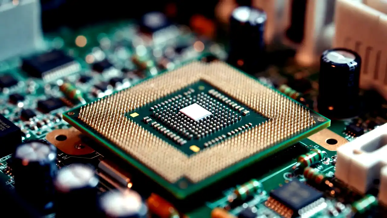
To solve the energy crisis, chipmakers cannot simply rely on traditional transistor scaling. Shrinking transistors using standard silicon materials has hit physical limitations, leading to severe issues with heat dissipation and current leakage. To continue boosting performance while dramatically lowering power consumption, the semiconductor industry must implement a highly integrated suite of architectural and material innovations.
Key Components of Next-Generation Chip Architectures
To achieve the extreme energy efficiency required by modern hyperscale data centers, chip manufacturers rely on five highly integrated, advanced technological systems:
- Advanced Logic Nodes (2nm and Below): Driving gate-all-around (GAA) transistor designs to shrink physical features, reduce operating voltage, and minimize current leakage.
- High-Bandwidth Memory (HBM): Stacking dynamic random-access memory (DRAM) dies vertically to bypass interconnect bottlenecks, boosting data transmission speeds while reducing power.
- 3D Stacking and Advanced Packaging: Using specialized bonders and precision etching to link separate chiplets with sub-3-micron pitch, allowing heterogeneous integration.
- Extreme Ultraviolet (EUV) Lithography: Using high-numerical-aperture patterning tools in line with advanced coater-developers to print atomic-level features.
- Green Manufacturing Systems: Reducing greenhouse gas emissions, water consumption, and chemical footprints across the physical tool supply chain.
Eliminating the Silicon Cycle: The Rise of the Semiconductor Super-Cycle
The massive capital expenditure wave triggered by the generative AI boom is also fundamentally altering the economics of the semiconductor industry. For decades, the global chip market was governed by highly volatile “silicon cycles”—turbulent boom-and-bust periods in which companies overproduced chips during periods of high demand, leading to severe supply gluts and sharp price crashes every three to four years.
Kawai and other leading industry executives believe that the explosive demand for AI servers is effectively erasing these traditional cyclical downturns. Instead of entering a standard corrective phase, the industry appears to be entering a prolonged, long-term “super-cycle” of surging demand. While capital investment in mature nodes has leveled off in some regions, investment in advanced-node manufacturing tools for generative AI applications is accelerating at an unprecedented rate.
Tokyo Electron’s Positive Financial Outlook
This economic shift has translated directly into historic financial gains for semiconductor equipment providers. Tokyo Electron has maintained a highly positive annual outlook, forecasting record-breaking revenues of 2.4 trillion yen (approximately $15.7 billion) for the fiscal year, representing an exceptional 31% year-over-year increase. The company’s operating profits are also projected to reach an all-time high of 680 billion yen, representing an extraordinary 49% annual growth rate.
To prepare for this prolonged super-cycle, Tokyo Electron is aggressively expanding its manufacturing capacity. The company announced plans to invest 104 billion yen (approximately $685 million) to build a state-of-the-art manufacturing facility for advanced circuit-etching equipment. This massive production expansion underscores the company’s expectation that AI-related capital spending will continue to rise throughout the decade, driving double-digit growth in the semiconductor equipment market beyond next year.
Korea-Japan Economic Solidarity: A Strategy for Global Survival
The transition to this advanced AI economy is also driving historic geopolitical shifts in East Asia. During the special session of the “Future of Asia” conference, business leaders, politicians, and academic experts agreed that closer economic collaboration between South Korea and Japan has become an absolute necessity for survival.
As the post-war global order faces severe challenges from rising trade protectionism, geopolitical conflicts, and technological rivalry between the United States and China, South Korea and Japan are moving to build a highly integrated tech alliance. Chey Tae-won, the Chairman of SK Group, proposed that the two neighboring nations should establish a highly institutionalized economic solidarity. He floated the bold idea of a $7 trillion shared economic bloc and an “AI alliance” between South Korea and Japan.
Building an AI Economic Bloc Cluster
Chey argued that by sharing data, standardizing technical standards, and building joint physical infrastructure, the two countries can secure their independent competitiveness amid the ongoing global tech wars. Mizuho Bank President Masahiko Kato strongly supported this plan, citing active examples of corporate cooperation in areas such as AI data centers, semiconductors, and liquefied natural gas (LNG).
Kawai also stressed the absolute importance of shared economic prosperity through a South Korea-Japan partnership. This collaboration makes perfect operational sense. South Korea dominates the global memory chip market through giants like Samsung Electronics and SK Hynix, which control the production of High-Bandwidth Memory (HBM) chips. Japan, on the other hand, dominates the supply of advanced chipmaking equipment and chemical materials through firms like Tokyo Electron and Shin-Etsu Chemical.
By linking Japan’s world-class toolmaking capabilities with South Korea’s dominant memory-fabrication plants, the two nations can build a highly resilient, unified supply chain insulated from external geopolitical shocks.
Technical Breakthroughs in Front-End Wafer Processing
To deliver on the promise of energy-efficient data centers, equipment manufacturers must execute highly precise breakthroughs at the atomic level during front-end wafer processing. This is the stage where microscopic electronic circuits are printed, etched, and cleaned on pure silicon wafers.
The Critical Role of Etching and Photoresist Coating
Tokyo Electron holds a dominant position in this highly specialized market, controlling approximately 90% of the global market share for photoresist coater/developer systems used in EUV lithography. The company’s tools are integrated in line with next-generation high-numerical-aperture (High-NA) EUV lithography systems.
These advanced coaters are highly compatible with spin-on metal-containing resists, which demonstrate exceptional resolution and high etch resistance compared to traditional chemically amplified resists. However, metal-containing resists require sophisticated control of pattern size and strict contamination control on the backside and bevel of the wafer.
Tokyo Electron’s advanced process modules solve these challenges by enabling a single unit to process multiple materials in-line. This technical capability realizes the high productivity, high yield, and high availability needed to make advanced chiplet architectures commercially viable.
Joint R&D for Next-Generation Scaling
To accelerate these breakthroughs, Tokyo Electron has extended its long-standing strategic research partnership with imec, a world-leading nanoelectronics research hub based in Belgium, for another five years. This renewed alliance focuses on co-developing tools and process technologies to support the next wave of semiconductor scaling beyond 2-nanometer nodes, specifically targeting advanced logic devices and 3D stacking.
Furthermore, the company extended its joint research agreement with IBM at the Albany NanoTech Complex in New York to co-develop chiplet architectures and advanced packaging processes. These research collaborations ensure that as chip nodes continue to shrink, the technology can meet the strict performance and energy efficiency requirements of the generative AI era.
Conclusion
The explosive rise of generative artificial intelligence has permanently altered the global technology landscape, placing the physical data center at the center of the modern economy. But as Tokyo Electron CEO Toshiki Kawai warned during the “Future of Asia” conference, the rapid expansion of these data centers cannot continue without massive advances in semiconductor energy efficiency. Perfecting advanced logic nodes, expanding high-bandwidth memory production, and developing precise front-end etching and coating tools have become absolute requirements to balance digital progress with global environmental preservation. As the traditional silicon cycle gives way to a prolonged, AI-driven super-cycle, closer economic solidarity among East Asian tech giants such as South Korea and Japan will serve as a vital engine for shared prosperity. By investing heavily in R&D and building highly resilient, green manufacturing systems, the semiconductor industry is working to ensure that the digital revolution remains sustainable, securing our technological future for generations to come.